





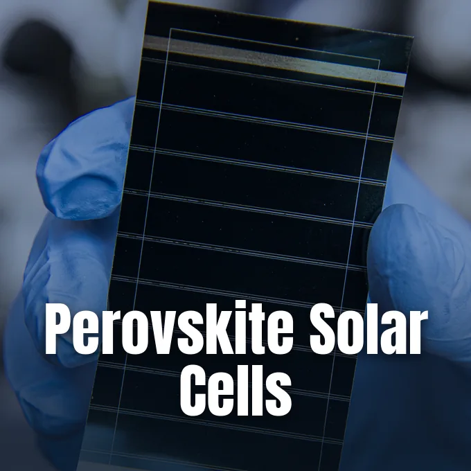
Perovskite solar cells are thin-film devices that use synthetic crystals to turn sunlight into electric power. Unlike classic silicon wafers that need furnace heat reaching 2000 °C in complex factories, metal-halide films assemble from liquid chemical inks at mild temperatures below 200 °C [1, 3]. Lab cell output rose from 3.8% in 2009 to over 27% today [1, 2]. Tandem prototypes built on silicon now exceed 34% [6, 7]. Oxford PV shipped test panels to an American utility site in 2024, but moisture decay and outdoor lifespan remain the main technical hurdles that researchers must resolve before wide deployment [4, 7].
Crystal Structure of the Absorber
The term perovskite comes from the mineral calcium titanate discovered in the Ural Mountains of Eurasia in 1839 and named after Russian nobleman Lev Perovski [4, 9]. At the National Renewable Energy Laboratory in Golden, Colorado, researchers classify these synthetic compounds by their shared crystal lattice rather than chemical ingredients [1, 9]. The atomic grid follows the formula ABX3, where A is a large monovalent cation, B is a divalent metal, and X is a halide anion [1, 7]. Corner-sharing metal-halide octahedra enclose the central cation inside a three-dimensional cubic cage [2, 12].
In practical devices, the A spot contains ions like methylammonium, formamidinium, or cesium, with ionic radii spanning 1.6 to 2.5 ångströms. The central B position holds lead, while the X corner binds iodide, bromide, or chloride [7, 12]. Halide adjustments let chemists tune light absorption across optical energy levels from 1.2 to 2.3 electron volts. Silicon stays locked at 1.1 electron volts [6]. Constantinos Stoumpos and Mercouri Kanatzidis showed that formamidinium lead trihalide lowers this bandgap toward optimal single-junction ranges [12]. At Northwestern University in Evanston, Illinois, materials scientist Robert Chang said that perovskite crystals assemble with ease in basic lab conditions, contrasting with the rigid lattice demands of silicon. Atomic flexibility lets crystals form clean grains without costly vacuum tools [2, 3].
Chemists also produce two-dimensional sheets like Dion-Jacobson phases. Mercouri Kanatzidis at Northwestern University and colleagues at Argonne National Laboratory showed that organic spacers isolate metal-halide sheets into stable crystal plates [17]. Interface control also gains from methods in the accelerated development of quantum dots, where automated synthesis refines colloidal surfaces to resist moisture penetration across exposed grain edges [2].
How Perovskite Solar Cells Generate Electricity
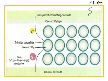
Perovskite solar cells turn sunlight into electricity through the photovoltaic effect investigated by Daniel Friedman and Jao van de Lagemaat at the National Renewable Energy Laboratory in Colorado [3, 11]. When photons strike the absorber, their energy knocks electrons from the valence band into the conduction band. This jump creates mobile negative charges and leaves behind positive holes [7, 11]. Because the exciton binding energy is low, charges free themselves without extra heat, creating mobile carriers that separate across internal energy offsets [10, 12].
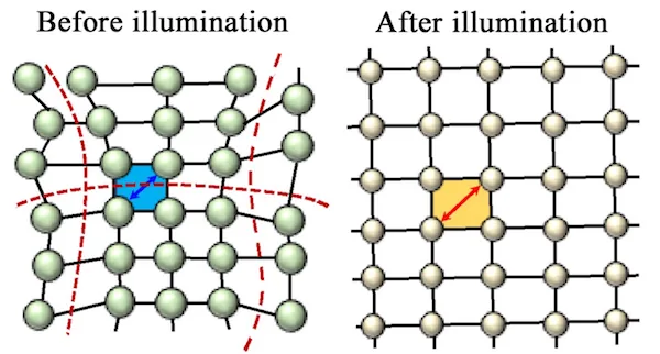
High optical absorption coefficients near 10^5 cm^-1 allow a crystal film only 300 to 500 nanometers thick to absorb as much sunlight as a silicon wafer measuring 150 to 200 micrometers [7, 10, 14]. Thin films use minimal raw material while gathering ample light [1, 10]. Unusually long diffusion paths let charges travel through the crystal without recombining too soon [3, 10]. Fast charge motion over wide optical bands connects with ideas seen in how light pulses transmit data across optical setups. At Los Alamos National Laboratory, chemist Aditya Mohite collaborated with Pulickel Ajayan and Rafael Verduzco at Rice University to show that lattice softness aids defect tolerance, preventing atomic slips from ruining charge collection [3, 14]. Silicon demands far purer crystal wafers to function [3]. Gentle light soaking even expands the lattice to assist carrier extraction [14].
Charge sorting depends on selective contact layers flanking the absorber. A tin oxide layer extracts negative electrons toward the front electrode while blocking positive holes, and an opposing polymer film simultaneously steers positive charges to the rear metal contact [7, 11]. Wired circuits allow these separated carriers to flow and power external electrical loads [5, 11].
Cell Architecture and Fabrication
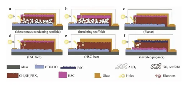
A working device stacks several thin layers on a rigid or bendable clear base [7, 9]. Processing starts on glass coated with fluorine-doped tin oxide or indium tin oxide [7, 10]. Workers lay an electron contact, the perovskite film, a hole collector like Spiro-OMeTAD, and an evaporated metal contact [7, 9]. Jao van de Lagemaat at the National Renewable Energy Laboratory in Golden, Colorado, said that balancing interface contacts decides overall power delivery [3].
Device designs follow two distinct architectures: regular n-type front stacks and reversed p-type bottom layouts. In standard n-i-p devices, the electron layer sits below the perovskite, taking light straight through the front glass. Reversed p-i-n layouts place the hole layer on the glass first [7, 9]. Data in Nature confirmed by teams at the University of Surrey Advanced Technology Institute show that inverted layouts hold up better under direct sun and heat [2, 5]. The absorber can form a smooth planar sheet or soak into a titanium dioxide scaffold [9, 11].
Making perovskite films avoids the huge energy footprint of silicon ingots that melt at heat levels near 2000 °C [3, 5]. Precursor salts dissolve in common liquid solvents to yield printable inks that engineers spread using spin-coating, slot-die heads, inkjet nozzles, or automated blade coaters at mild heat below 150 °C [2, 5, 11]. At KAUST and Helmholtz-Zentrum Berlin in Germany, teams blade-coated cells yielding 31.2% efficiency [5]. Thermal vapor deposition in vacuum chambers provides another path for coating wide surfaces [2].
Silicon Single-Junction Limits
Single-junction silicon limits were calculated in 1961 by William Shockley and Hans-Joachim Queisser at Bell Labs. The Shockley-Queisser limit shows that a single junction with a 1.1 electron volt bandgap can’t exceed 33.7% solar conversion. Silicon loses significant power because low-energy infrared rays pass straight through unabsorbed, while higher-energy photons waste excess energy as heat, leaving commercial silicon panels capped between 22% and 24% efficiency [6, 7, 12].
Perovskite films escape these boundaries through tunable bandgaps and bright light response [6, 12]. Formamidinium lead trihalide reaches a bandgap near 1.48 electron volts, close to the ideal 1.34 value for peak single-cell output [12]. In a study in Science, Aditya Mohite and Wanyi Nie at Los Alamos National Laboratory and Rice University in Houston discovered that steady sunlight relaxes mechanical strain in the crystal lattice. Reza Asadpour and Muhammad Ashraf Alam at Purdue University modeled these carrier dynamics, proving that atomic relaxation lowers contact resistance and lifts cell output from 18.5% to 20.5% without heat decay over 1,500 hours. Strain relief lasted thirty minutes in the dark [14].
Efficiency progress moved faster than any prior solar material [2, 3]. In 2009, Tsutomu Miyasaka at Toin University of Yokohama built the first cell at 3.8% [3, 5]. Nam-Gyu Park developed solid-state cells that reached 9.7% efficiency in 2012 [2, 6, 12]. Certified lab cells at the National Renewable Energy Laboratory in Colorado now exceed 27% [7, 11]. Silicon needed fifty years for that leap [12].


Tandem Perovskite Solar Cells with Silicon
Tandem setups pair two semiconductors to harvest separate slices of the solar spectrum within one panel [6, 8]. A perovskite top cell absorbs energetic blue and green light. Lower-energy red and infrared light passes into a silicon bottom cell, which absorbs it cleanly [7, 8]. Spectral splitting cuts thermalization losses and lifts the theoretical ceiling past 45% [4, 12]. Henry Snaith at the University of Oxford said stacking these materials unlocks extra power without replacing established silicon lines [3, 4].
Engineers link tandem cells through two-terminal monolithic bonds or four-terminal stacked mountings. Two-terminal designs join the perovskite and silicon layers in series with a central joint [6, 12]. This layout cuts wiring and module weight. But two-terminal tandems demand matched currents between both layers, so uneven shade limits output. Four-terminal tandems run each cell on separate circuits, dodging current limits while using extra clear electrodes [6, 12]. Scott Graybeal at Caelux, established through Caltech laboratory research, said independent circuits give flexibility for specialized vehicles [4].
Lab records for tandem cells have broken the single-silicon ceiling. In 2024, Oxford PV hit a certified 33.9% cell mark, while Chinese maker LONGi posted a 34.85% record [6, 7]. Trinasolar in Changzhou demonstrated tandem cells reaching 31.1% efficiency. Oxford PV also built full-size home modules yielding 26.9% [4, 7]. For a home rooftop with twenty panels, lifting panel output from 22% to 23% adds roughly 80 peak watts with no extra roof mounts, trimming balance-of-system installation costs across residential arrays [6].
Why the Cells Degrade Outdoors
Why do perovskite panels degrade faster than silicon when placed under open skies? The vulnerability stems from chemical weakness in the crystal lattice [6, 7]. Moisture poses the most severe threat because penetrating water molecules hydrolyze hygroscopic organic cations like methylammonium, breaking down the lead-halide crystal cage and converting black photoactive absorber films into inert yellow lead iodide [2, 7, 12]. Air oxygen worsens this breakdown by forming reactive superoxides under light [15]. Laura Miranda and David Ward at Oxford PV test this moisture risk inside environmental climate chambers [4].
Can heat and ultraviolet rays cause similar damage to bare cells? Sun heat drives organic vapors out of the lattice, creating pinholes and deep trap states [2, 6]. In inorganic cesium lead iodide, heat causes the black alpha phase to flip into a yellow delta phase at room temperatures. Moving ions under electric fields also distort current-voltage scans, producing hysteresis that skews lab tests [11, 12]. Joseph Berry at the National Renewable Energy Laboratory said module longevity remains the key material science question that requires long-term outdoor data [4].
To stop decay, module builders use edge sealants and glass barriers [1, 7]. Teams also build two-dimensional caps over the perovskite film [2, 17]. Research in the Journal of the American Chemical Society showed that oily organic cations build sheets that stop water entry [17]. Mixing formamidinium with cesium gives greater heat stability, helping test cells keep 95% initial output after 2,000 hours of continuous light at City University of Hong Kong [2, 5]. Teams at the University of Surrey Advanced Technology Institute extended operational lifetimes by 66% using chemical passivators [5]. Accelerated aging chambers simulate years of sun exposure in months [4]. Moisture seals protect delicate layers [1, 7].
Lead Toxicity and Alternative Metals
Lead content inside high-performing perovskite solar cells creates recognized health and environmental hurdles because toxic heavy metals can damage human nervous systems and natural biological food chains [5, 12]. If hail or fire cracks a fielded module, rainwater could dissolve lead salts into local soil [12, 13]. European Union regulations like the RoHS directive restrict hazardous electronics, and while solar panels hold temporary exemptions, long-term market trust requires certified recycling frameworks across utility programs [4, 6]. David Ward at Oxford PV said panels are designed for standard recycling streams. Joseph Berry at the National Renewable Energy Laboratory in Colorado noted that end-of-life recycling procedures can safely isolate heavy metals from damaged hardware [4].
Tin offers the main lead-free choice within group 14 of the periodic table [13, 16]. In Energy & Environmental Science, Noel and Henry Snaith at the University of Oxford built the first lead-free methylammonium tin iodide cell, hitting over 6% output and 0.88 volts from a 1.23 electron volt bandgap [16]. But tin oxidizes swiftly. The divalent tin ion flips to tetravalent tin when meeting air or moisture. That shift creates background defects and triggers carrier loss, cutting power. Tin-based absorbers like FASnI3 deliver a 1.3 electron volt bandgap, but ambient oxygen triggers rapid defect growth [13, 15].
Chemists slow tin decay with tin fluoride and fullerene additives [13, 15]. In Nature Photonics, Zhanhua Wei at Huaqiao University used trans-isomeric fulleropyrrolidine additives to guide crystal growth, reaching 15.38% output while holding 93% power after 500 hours under light [15]. Triple-cation tin cells reached 16.65%. Lead-free designs offer a clean path forward [12, 13].
Perovskite Solar Cells at Commercial Scale
Factory scale-up for perovskite photovoltaics brings real production challenges [5, 8]. Record lab scores reported by the U.S. Department of Energy Integrated Energy Systems Office happen on tiny test chips measuring 0.1 to 1 square centimeter [1, 6]. Utility panels need even coats over 1.6 square meters. Uniform film coating across large substrates without pinholes is difficult [6, 8]. Laser scribing lines to link cells adds dead space and cuts active power area [1, 8].
Field testing hit a milestone in September 2024 when Oxford PV sent tandem panels to an American utility customer. Built at a plant in Brandenburg, Germany, these pilot panels yield 24.5% module efficiency. The firm targets volume production for 2027, while Swift Solar, a spinout from Stanford University and the Massachusetts Institute of Technology, expands pilot lines and Caelux in the United States [4, 7, 8]. In China, GCL Group Holdings began building a large factory in Suzhou, Trinasolar posted a 31.1% tandem lab mark, and LONGi claimed 33.9% on a single tandem cell [4, 5]. Japan’s Ministry of Economy, Trade and Industry plans 20 gigawatts of perovskite capacity by 2040 [5].
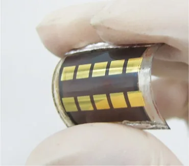
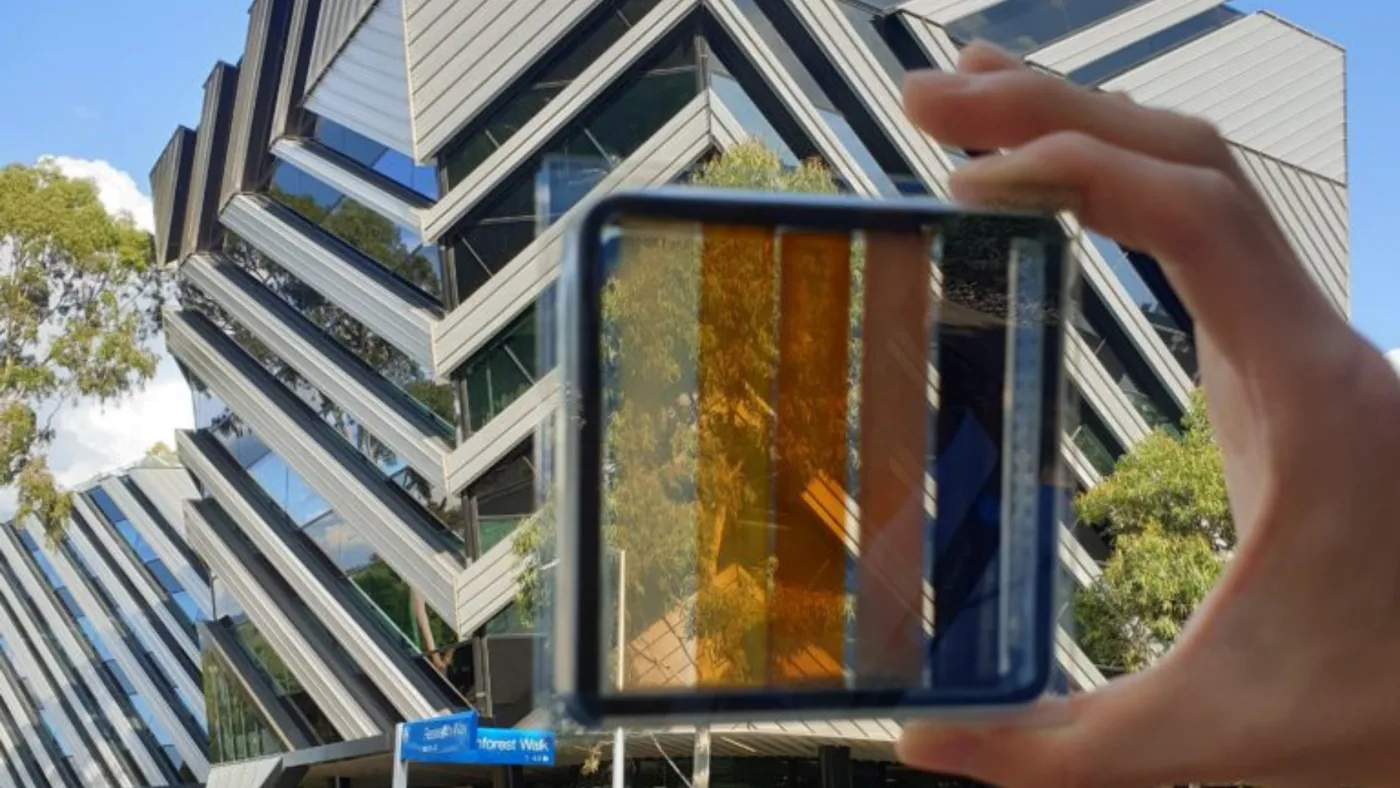
Beyond rooftop grids, bendable and semi-transparent perovskite films suit unusual power uses. Lightweight films fit curved electric car roofs, portable chargers, and see-through solar windows [5, 11]. In low-power electronics, Sai Nithin Kantareddy and Tonio Buonassisi at the Massachusetts Institute of Technology ran a wireless sensor using a 10.1% perovskite module, as reported in an un-peer-reviewed arXiv preprint [18]. Swift Solar and American Tower Corporation also piloted panels on telecom towers [4]. Field data will determine when warranties match silicon [6, 8].
- WEBSITE U.S. Department of Energy. (2015). Perovskite Solar Cells. Integrated Energy Systems Office. [Article Link]
- ACADEMIC JOURNAL Han, J., Park, K., Tan, S., Vaynzof, Y., Xue, J., Diau, E. W.-G., Bawendi, M. G., Lee, J.-W., & Jeon, I. (2025). Perovskite solar cells. Nature Reviews Methods Primers, 5(1). [Article Link]
- ONLINE NEWS Hamers, L. (2017). Perovskites power up the solar industry. Science News Magazine. [Article Link]
- ONLINE NEWS Early, C. (2025). Perovskite: The ‘wonder material’ that could transform solar. BBC Future. [Article Link]
- ONLINE NEWS Shaikh, K. (2024). Perovskite solar cells: Explaining the next big thing in solar. Interesting Engineering. [Article Link]
- WEBSITE SurgePV. (2026). Perovskite Solar Technology: Next-Gen Cells. [Article Link]
- WEBSITE Lozanova, S. (2026). Perovskite Solar Cell vs. Silicon: Working Principle & 2026 Outlook. GreenLancer. [Article Link]
- WEBSITE Çay, M. (2026). Perovskite Solar Cells Explained: The 2026 Reality Check. Solarsunlabs. [Article Link]
- ONLINE NEWS Solar Magazine. (2022). Perovskite Solar Cells: An In-Depth Guide + Comparisons With Other Techs. [Article Link]
- WEBSITE RF Wireless World. (2026). Perovskite Solar Cells: Promising Tech or Environmental Hazard? [Article Link]
- WEBSITE HowAtlas. (2026). How Perovskite Solar Cells Work: Advancing Photovoltaic Efficiency. [Article Link]
- WEBSITE Wikipedia. (2026). Perovskite solar cell. Wikimedia Foundation. [Article Link]
- WEBSITE Wikipedia. (2026). Tin-based perovskite solar cell. Wikimedia Foundation. [Article Link]
- PRESS RELEASE Rice University. (2018). Light ‘relaxes’ crystal to boost solar cell efficiency. Rice News. [Article Link]
- ACADEMIC JOURNAL Chen, J., Luo, J., Hou, E., Song, P., Sun, Y., Feng, C., Zhang, W., Xie, S., Tian, H., & Wei, Z. (2024). Efficient tin-based perovskite solar cells with trans-isomeric fulleropyrrolidine additives. Nature Photonics, 18, 464–470. [Article Link]
- ACADEMIC JOURNAL Noel, N. K., Stranks, S. D., Abate, A., Wehrenfennig, C., Guarnera, S., Haghighirad, A. A., Sadhanala, A., Eperon, G. E., Pathak, S. K., Johnston, M. B., Petrozza, A., Herz, L. M., & Snaith, H. J. (2014). Lead-free organic–inorganic tin halide perovskites for photovoltaic applications. Energy & Environmental Science, 7(9), 3061–3068. [Article Link]
- ACADEMIC JOURNAL Mao, L., Ke, W., Pedesseau, L., Wu, Y., Katan, C., Even, J., Wasielewski, M. R., Stoumpos, C. C., & Kanatzidis, M. G. (2018). Hybrid Dion–Jacobson 2D Lead Iodide Perovskites. Journal of the American Chemical Society, 140(10), 3775–3783. [Article Link]
- PREPRINT Kantareddy, S. N. R., Mathews, I., Sun, S., Layurova, M., Thapa, J., Correa-Baena, J.-P., Bhattacharyya, R., Buonassisi, T., Sarma, S. E., & Peters, I. M. (2019). Perovskite PV-powered RFID: enabling low-cost self-powered IoT sensors. arXiv. [Article Link]


