





How transistors work comes down to a simple physical principle: a weak electric signal applied to a control terminal dictates how much current can pass between two other terminals. By altering the electric conductivity of a semiconductor material like silicon, the device acts as a switch that turns an electric flow on and off, or as an amplifier that strengthens faint incoming waves. Because solid semiconductor crystals handle this regulation without moving mechanical pieces or fragile vacuum chambers, transistors provide dependable electronic control over millions of operating hours [1]. Before solid-state electronics took shape, engineers relied on glass vacuum tubes that ran hot, burned out regularly, and drew large amounts of power. Today, computer makers pack billions of microscopic transistors onto single silicon chips that fit neatly on a fingertip. Understanding how transistors work clarifies how a simple physical effect became the bedrock of modern computing [3].
How Transistors Work as Electronic Switches
Pure silicon is not an efficient conductor because its four valence electrons form tight bonds within the crystal lattice, leaving few free charge carriers to move electricity. To change this behavior, chip makers introduce minute impurities into the crystal through a chemical process called doping. Adding elements with five valence electrons, like phosphorus or arsenic, provides extra mobile electrons that create an n-type semiconductor where negative charges move freely under an electric field. In contrast, adding elements with three valence electrons, like boron, leaves empty spaces known as electron holes. These holes create a p-type semiconductor where positive charges appear to flow as neighboring electrons shift into vacant positions [2].
When p-type and n-type silicon meet, they form a boundary known as a p–n junction. Near this interface, free electrons wander past the boundary to fill nearby holes, creating a narrow depletion region stripped of mobile carriers that naturally resists further electrical flow. Applying a control voltage disrupts this internal balance, either widening the barrier to block passage or flattening it so current surges through the channel. This mechanism explains how transistors work as binary switches. A positive gate voltage creates a conductive highway that represents a logical one, while removing the voltage cuts the flow to represent a logical zero [1].
Why do computer chips generate so much heat as they process data? Every time charge carriers rush through the channel resistance, tiny pulses of thermal energy escape into the silicon substrate. If billions of miniature gates switch at the same time, that accumulated heat can cause errors or degrade hardware life [9].

The Move Away From Vacuum Tubes
Early radio transmitters and telephone lines relied on the thermionic triode, a vacuum tube invented in 1907 that could amplify faint signals. But triodes were fragile, bulky, and consumed large quantities of power just to heat their internal filaments. In 1925, Polish-American physicist Julius Edgar Lilienfeld patented the basic concept of a field-effect device using copper sulfide, followed by German engineer Oskar Heil, who patented a capacitive control scheme in 1934. Neither inventor could construct a working prototype at the time, mostly because nobody knew how to prepare semiconductor materials with sufficient purity [10].
The crucial practical breakthrough came at Bell Labs in Murray Hill, New Jersey, during the closing months of 1947. Working under solid-state physics leader William Shockley, physicists John Bardeen and Walter Brattain pressed two closely spaced gold foil contacts onto a rough crystal of germanium. On December 23, 1947, they observed that a small input signal produced an amplified output wave, proving that a solid crystal could replace a vacuum tube. Bell engineer John R. Pierce coined the term transistor as a contraction of transresistance, and Shockley, Bardeen, and Brattain later shared the 1956 Nobel Prize in Physics for their discovery [1].
In Europe, German physicists Herbert Mataré and Heinrich Welker pursued similar experiments for a Westinghouse subsidiary in France. Drawing on wartime radar work, they noticed that two point contacts placed within 100 micrometers on germanium produced signal interference. Mataré obtained steady amplification by June 1948 using high-purity germanium prepared by Welker, patenting the device as the transistron before junction models replaced point contacts [11].
How Bipolar Transistors Work
Why do discrete transistors require three separate leads rather than two? The answer lies in how charge carriers move through distinct semiconductor layers. A bipolar junction transistor, or BJT, consists of three alternating regions arranged in either an NPN or a PNP sandwich, with terminals labeled emitter, base, and collector [2].
In a standard NPN transistor, the middle base layer is fabricated to be exceptionally thin and lightly doped, while the emitter is heavily doped with donor atoms that supply abundant free electrons. The collector layer is doped more lightly than the base to withstand reverse voltages. To turn the device on, an external circuit applies a small forward bias of roughly 0.7 volts across the base-emitter junction. This input lowers the internal potential barrier and injects a swarm of electrons from the emitter into the thin base region [2].

Because the base region is so narrow, most of the injected electrons do not recombine with local holes; instead, they drift straight into the depletion zone of the reverse-biased collector junction, where a strong electric field sweeps them into the collector circuit. A tiny current flowing into the base thereby unleashes and regulates a much larger current between the collector and the emitter. This current-controlled behavior makes BJTs effective analog amplifiers for audio equipment and radio receivers, though their continuous base current draws more energy than modern digital processors can afford [2].
How Field-Effect Transistors Work
Unlike bipolar devices that need an ongoing input current, a field-effect transistor operates as a voltage-controlled switch that draws virtually zero continuous current at its control terminal. William Shockley outlined the theory of the junction field-effect transistor in 1952, and engineers George C. Dacey and Ian M. Ross built the first working JFET in 1953 [4].
Early field-effect experiments struggled with surface defects that trapped electrons and prevented electric fields from penetrating into the underlying semiconductor. In 1955, Bell Labs scientists Carl Frosch and Lincoln Derick discovered by accident that heating a silicon wafer in an oxygen-rich furnace produced a thin, resilient layer of silicon dioxide. This glass-like coating passivated the surface, protected the delicate crystal from contaminants, and served as an impermeable barrier against unwanted dopant diffusion, opening a path toward durable planar manufacturing [1].
Building on that oxidation technique, Mohamed Atalla and Dawon Kahng constructed the first metal-oxide-semiconductor field-effect transistor, or MOSFET, at Bell Labs in 1960. A modern MOSFET places an insulating oxide layer between a gate terminal and the silicon channel that connects the source and drain. When a positive voltage is applied to the gate of an n-channel device, the electric field attracts electrons toward the oxide interface, creating a conductive inversion layer that lets current pass. Because the gate stays insulated by the oxide, the transistor draws power only when switching states, making it the most energy-efficient switch in history [1].


The Regency TR-1 Radio
Although Bell Labs invented the transistor in 1947, consumer electronics companies hesitated to adopt the expensive components in place of proven vacuum tubes. That hesitation ended in 1954 when Texas Instruments teamed up with Industrial Development Engineering Associates, known as I.D.E.A., to create the first commercial pocket transistor radio. Manufactured in Indianapolis, Indiana, under the Regency brand, the Regency TR-1 reached store shelves on October 18, 1954, priced at $49.95, and ran on a single 22.5-volt battery that delivered more than twenty hours of continuous listening [13].
Early prototype radios required technicians to manually test and match individual transistors to make circuits work, which drove unit costs far too high for mass retail. Regency engineer Dick Koch solved this manufacturing barrier by designing a clever feedback circuit that accommodated wide component tolerances, allowing standard assembly line workers to solder transistors directly onto circuit boards without prior sorting. Thanks to Koch’s circuit layout, Regency built and sold roughly 140,000 radios, proving that solid-state consumer products could be manufactured at commercial volume [13].
The pocket-sized TR-1 kicked off a cultural shift by letting listeners take music and news outside the home. Apple co-founder Steve Wozniak later pointed to the Regency radio as an early inspiration, stating, “I loved what it could do, it brought me music, it opened my world up.” Without portable transistor hardware, personal computers and modern smartphones might never have appeared [14].

CMOS Logic in Microprocessors
In 1963, Chih-Tang Sah and Frank Wanlass at Fairchild Semiconductor introduced complementary metal-oxide-semiconductor logic, commonly known as CMOS. By pairing n-channel and p-channel MOSFETs in a push-pull arrangement, CMOS circuits draw measurable current only during the momentary transition when switching between logical high and low states. One transistor is always turned off while the other is turned on, virtually eliminating static power leakage. This configuration reduced circuit power demands so significantly that engineers could pack thousands, and eventually millions, of logic gates onto a single piece of silicon [1].
The arrival of monolithic integrated circuits led directly to the central processing unit on a chip. When Intel released the 4-bit Intel 4004 in 1971, the entire microprocessor fit onto a single silicon die holding 2,300 transistors. Seven years later, the 16-bit Intel 8086 processor contained 29,000 transistors [3].
As semiconductor fabrication advanced, reducing transistor gate dimensions yielded major gains in operating frequency and energy efficiency. For example, AMD transitioned its quad-core Phenom II desktop processor from a 65-nanometer process to a 45-nanometer node code-named Deneb. That die shrink increased the processor’s transistor count from roughly 450 million to 758 million while cutting power consumption, allowing flagship models like the Phenom II X4 940 Black Edition to run comfortably at 3.0 GHz on standard motherboard sockets [9].
Trillion-Transistor Chips and Density Records
Modern chip foundries no longer build computers out of flat planar transistors, switching instead to 3D FinFET and gate-all-around architectures where conductive channels are wrapped in thin silicon fins to prevent electrical leakage. This structural leap allowed Cerebras Systems to manufacture the Wafer Scale Engine 2, an AI processor carved out of an entire silicon wafer using a 7-nanometer process. Spanning 84 interconnected die fields, the Cerebras chip contains 2.6 trillion MOSFETs on a single piece of silicon, setting a record for monolithic computational hardware [3].
Data storage hardware has pushed physical transistor counts even higher by building microscopic memory cells vertically. In flash memory, Micron developed a 2-terabyte, 16-die chip featuring a 232-layer V-NAND design that packs 5.3 trillion floating-gate MOSFETs into a compact package [3].

Consumer microprocessors and graphics accelerators continue to register massive hardware density numbers. Nvidia built its Rubin accelerator on TSMC’s custom N3P process, assembling 336 billion MOSFETs on a single processing unit. In the consumer space, Apple’s dual-die M3 Ultra system-on-chip incorporates 184 billion transistors fabricated on a 3-nanometer node. Worldwide, historians estimate that humanity has manufactured more than 1.3×10²² transistors, making the solid-state switch the most multiplied physical object in human history [3].
Electrochemical and Fluidic Alternatives
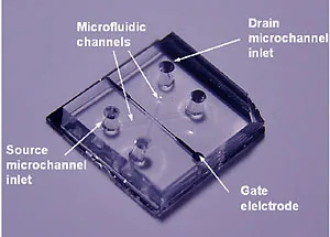
While silicon remains the standard foundation for commercial computer chips, researchers are designing non-silicon devices that can operate in fluids or biological tissues. At the University of California, Berkeley, Arun Majumdar and Peidong Yang built a nanofluidic transistor that regulates the movement of potassium ions through water-filled channels measuring just 35 nanometers in height. By applying an electrical voltage between silicon dioxide plates, the researchers could pinch off ion migration, proving that chemical solutions can mimic electronic switching for early cancer screening and DNA sorting [5].
At Harvard’s John A. Paulson School of Engineering and Applied Sciences, a research team led by Woo-Bin Jung developed an aqueous ionic processor in collaboration with biotech startup DNA Script. Their device arranges hundreds of ionic transistors in a 16 × 16 matrix submerged in a quinone solution, performing analog multiply-accumulate operations in water for neural net computing [16].
Other teams are turning everyday organic substances into functioning switches. At Linköping University, researchers created a wooden electrochemical transistor using balsa wood treated to remove lignin before coating the cellulose tubes with a conducting polymer called PEDOT:PSS. The three-centimeter device switches at less than one hertz, offering a biodegradable switch that could monitor living plant health. Meanwhile, at Universidade Nova de Lisboa, Elvira Fortunato showed paper-based transistors where cellulose acts as a functional dielectric layer, proving that alternative materials continue to expand transistor applications in unexpected environments [6].
- WEBSITE Wikipedia contributors. (2026). Transistor. Wikipedia, The Free Encyclopedia. [Article Link]
- WEBSITE Wikipedia contributors. (2026). Bipolar junction transistor. Wikipedia, The Free Encyclopedia. [Article Link]
- WEBSITE Wikipedia contributors. (2026). Transistor count. Wikipedia, The Free Encyclopedia. [Article Link]
- BOOK CHAPTER Nishizawa, J. (1982). Junction Field-Effect Devices. In R. Sittig & P. Roggwiller (Eds.), Semiconductor Devices for Power Conditioning (pp. 241-268). Plenum Press. [Article Link]
- PRESS RELEASE Sanders, R. (2005, June 28). Researchers create first nanofluidic transistor, the basis of future chemical processors. UC Berkeley Media Relations. [Article Link]
- ONLINE NEWS Genkina, D. (2023, April 29). Timber! The world’s first wooden transistor. IEEE Spectrum. [Article Link]
- ONLINE NEWS IEEE Spectrum. (2008, September 1). Paper transistor. IEEE Spectrum. [Article Link]
- ONLINE NEWS Pires, F. (2022, October 5). Water-based chips could be breakthrough for neural networking, AI. Tom’s Hardware. [Article Link]
- ONLINE NEWS Toepelt, B., & Völkel, F. (2009, January 8). AMD Phenom II X4: 45nm benchmarked. Tom’s Hardware. [Article Link]
- WEBSITE Computer History Museum. (2007). 1926: Field effect semiconductor device concepts patented. The Silicon Engine. [Article Link]
- WEBSITE Computer History Museum. (2003). 1948: The European transistor invention. The Silicon Engine. [Article Link]
- ONLINE NEWS Die Welt. (2008, November 14). Der deutsche Erfinder des Transistors. Die Welt. [Article Link]
- WEBSITE Regency TR-1 Online Museum. (1997, October 30). Regency TR-1 transistor radio history. [Article Link]
- BOOK Wrobbel, E. (2021). The Regency TR-1 Family: The complete guide to the Regency TR-1 and related transistor models. [Article Link]
- ACADEMIC JOURNAL Tran, V. C., Mastantuoni, G. G., Zabihipour, M., Li, L., Berglund, L., Berggren, M., Zhou, Q., & Engquist, I. (2023). Electrical current modulation in wood electrochemical transistor. Proceedings of the National Academy of Sciences, 120(18). [Article Link]
- ACADEMIC JOURNAL Jung, W., Jung, H. S., Wang, J., Hinton, H., Fournier, M., Horgan, A., Godron, X., Nicol, R., & Ham, D. (2023). An aqueous analog MAC machine. Advanced Materials, 35(37). [Article Link]


