






Hardware leaker Kepler_L2 revealed on NeoGAF forums that early silicon for the next-generation PS6 chip and Microsoft’s upcoming Xbox Project Helix has reached the manufacturing tape-out stage. The leak, quickly spotted by VideoCardz and WCCFTech, outlines preliminary GPU compute targets while detailing manufacturing milestones for both competing systems. Tape-out indicates that physical layout blueprints have been completed and officially delivered to semiconductor fabrication facilities for initial prototype production runs [1].
Tape-Out Milestones for the PS6 Chip
Reaching the tape-out milestone indicates that engineers have finished the physical layout design of an integrated circuit and submitted it to the foundry for initial validation runs. This transition suggests both Sony and Microsoft are making tangible hardware progress toward the next console generation. Kepler_L2 noted that if tape-out has genuinely occurred, next-generation hardware could track toward a late-2027 release window [1]. TechRadar writer David Nield countered that commercial retail availability may still slip into 2028 because silicon validation and system testing require extensive operational cycles [2].
Neither platform manufacturer has officially confirmed the leaked production schedule or technical architecture blueprints. KitGuru editor João Silva emphasized caution regarding these early development milestones, noting in his coverage: “As always with early console rumours, these figures should be treated cautiously”. Kepler_L2 pointed out that early console SoCs undergo iterative hardware revisions as silicon testing progresses before entering volume production. KitGuru reported that Microsoft’s approach to system design remains largely unknown [1].
Both gaming systems reportedly rely on customized architectures combining AMD Zen 6 central processor cores with RDNA 5 graphics hardware, establishing a unified architectural foundation for the upcoming console generation [2]. Sony’s custom silicon engineering has historically prioritized proprietary security measures and dedicated subsystem co-processors, an architectural lineage previously explored when the PlayStation 2 security chip fell to independent reverse engineering [1]. Integrating Zen 6 processor cores will substantially improve instruction throughput, branch prediction, and multi-threaded calculations across demanding gaming workloads and operating system background tasks [2]. Furthermore, semiconductor fabrication engineers at foundry facilities must now validate whether early prototype wafers can consistently sustain projected clock frequencies without triggering thermal throttling during prolonged operational stress testing cycles [1].

PS6 Silicon and RDNA 5 Compute Units
Hardware specifications detailed on NeoGAF explain the physical silicon configuration planned for the upcoming PlayStation graphics processor. The PS6 chip architecture reportedly incorporates 54 RDNA 5 compute units fabricated on advanced foundry process nodes. Chris Harper reported for HotHardware on Wednesday, September 23, 2026, at 03:11 PM EDT that Sony intends to clock these active compute units between 2.6GHz and 3.0GHz. Operating across those target frequencies produces a theoretical compute throughput of 40 TFLOPS. Sony disabled two compute units [3].
Kepler_L2 noted that the 40 TFLOPS figure reflects theoretical FMA (Fused Multiply-Add) calculation throughput rather than real-world rendering speed. Sony targets 40 TFLOPS [1].
What chip will PS6 use to bridge this generational divide? TweakTown performance documentation indicates that the base PlayStation 5 delivers 10.28 TFLOPS, while the mid-generation PlayStation 5 Pro achieves 16.7 TFLOPS during typical operation and reaches 18.05 TFLOPS at peak compute capacity [2]. Moving to a 40 TFLOPS baseline on the PS6 chip effectively quadruples the theoretical compute capacity of the original 2020 launch hardware [3]. Kepler_L2 clarified that floating-point metrics reflect raw mathematical calculation capacity rather than guaranteed in-game performance [1].


Xbox Helix Chip Targets a 56 TFLOPS Ceiling
Microsoft’s next-generation console, internally codenamed Project Helix, adopts a noticeably larger silicon footprint housing 68 RDNA 5 compute units. Chris Harper noted that these 68 compute units will feature core clock speeds starting at 2.5GHz, generating roughly 56 TFLOPS of theoretical FP32 performance. That compute budget gives Microsoft a forty percent theoretical floating-point advantage over Sony’s 40 TFLOPS baseline. The gap reaches 16 TFLOPS. A thread participant on NeoGAF suggested the PS6 could exceed NVIDIA’s GeForce RTX 5080 through dual-issue compute, though Kepler_L2 declined to endorse that specific comparison [3].
Historical console generation launches demonstrate that a raw numerical compute advantage does not automatically translate into superior visual presentation on consumer displays. When the ninth console generation arrived in 2020, Microsoft’s Xbox Series X carried a 20% edge on TFLOPS over the PlayStation 5, registering 12.15 TFLOPS against Sony’s 10.28 TFLOPS. That prior advantage rarely yielded dramatic visual divergences in multiplatform titles [2]. Compiler efficiency dictated visual presentation [3].

HotHardware provided broader context by charting compute metrics across the console landscape. The portable Nintendo Switch 2 generates 3.072 TFLOPS in docked mode and 1.71 TFLOPS in handheld mode, while Microsoft’s entry-tier Xbox Series S delivers 4.006 TFLOPS. Switch 2 pairs low-power Arm processor cores with specialized NVIDIA graphics architecture to produce competitive gaming experiences despite a constrained mobile power envelope. Chris Harper charted these platforms [3].
Architectural Efficiency Beyond Raw Compute Numbers
Technical hardware analysis repeatedly confirms that teraflop ratings represent an incomplete measure of real-time 3D rendering capability. HotHardware highlighted empirical benchmarks from Digital Foundry proving that “your FPS-per-teraflop can increase by as much as 60% despite the same ‘raw’ compute number” [3]. Memory bandwidth constraints, cache hierarchies, and dedicated ray tracing silicon substantially dictate how many rendered frames reach the player’s television screen [1]. Architectural balance outweighs raw mathematics [3].
Early supply chain reports indicate Sony may equip the PS6 chip with GDDR7 memory, providing substantially wider memory bandwidth to feed its 54 RDNA 5 compute units [1]. Industry discussion cited by TechRadar points to 30GB of unified system RAM for the upcoming Sony machine, whereas Microsoft’s planned memory capacity for Project Helix remains unrevealed. Sony regularly enhances peripheral hardware to complement its core system silicon, as seen when PS5 Pulse headsets gained custom planar magnetic audio drivers [2]. Higher memory bandwidth prevents computational stalls during complex ray tracing calculations [1].
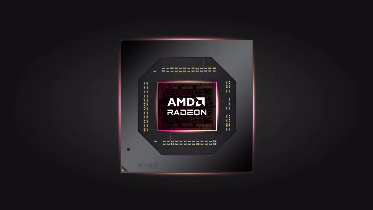
Development studios must decide how extensively they will tailor rendering engines to exploit Project Helix’s 68 compute units. Multiplatform software teams typically optimize core rendering loops around baseline console hardware before applying dynamic resolution scaling and framerate unlocks for higher-tier platforms. If game developers establish the 40 TFLOPS PS6 chip as their primary technical baseline, Project Helix may primarily deliver higher native display resolutions rather than fundamentally redesigned game mechanics. Technical compromises guide multiplatform deployment [3].
Memory Costs and Projected Release Windows
Gaming communities on Reddit have reacted to these leaked hardware specifications with immediate concern regarding retail pricing. Rather than celebrating the theoretical TFLOPS figures, enthusiast discussions focused heavily on estimated fabrication expenses, with one forum participant warning of “an inevitably massive price hike”. Another commenter argued that consumers should prepare to “say goodbye to affordable console hardware” as cutting-edge silicon manufacturing costs continue to escalate across advanced foundry nodes. Forum members voiced persistent apprehension [2].
Recent consumer hardware launches demonstrate that persistent memory component shortages drive retail prices upward across the gaming industry, a trend previously observed with the Steam Machine. Packing 30GB of high-speed memory with multi-die semiconductor packaging could push both Sony and Microsoft into unprecedented launch price tiers. Players awaiting next-generation machines will spend the intervening years exploring major releases including Grand Theft Auto 6 on existing PlayStation 5 and Xbox Series X consoles. David Nield tracked memory inflation [2].
Production schedules remain tentative while early silicon wafers navigate laboratory evaluation. If the leaked tape-out milestone proves accurate, the physical PS6 chip will undergo rigorous testing over upcoming quarters as engineers measure thermal output and real-world clock stability [1]. Whether commercial hardware arrives in late 2027 or slips into 2028, both platform holders have established their foundational silicon targets for the approaching console generation. Foundry testing will verify 3GHz clocks [3].
- ONLINE NEWS Silva, J. (2026, September 24). Leaker claims chips for PS6 and Xbox Helix are ‘taped out’. KitGuru. [Article Link]
- ONLINE NEWS Nield, D. (2026, September 24). A leaker says the chips in the PS6 and Xbox Helix have been finalized, and there’s a big power difference between them — but it’s the likely price jump that gamers are mostly talking about. TechRadar. [Article Link]
- ONLINE NEWS Harper, C. (2026, September 23). Xbox Helix Leak Tips 56 TFLOPS GPU To Overpower PS6 By 40%. HotHardware. [Article Link]


