




Benchmark listings from the Geekbench database have revealed the first performance numbers for AMD Medusa Point engineering samples, showcasing generational gains over current Ryzen mobile chips. The leaked submissions cover early test silicon running on internal evaluation boards and prototype Lenovo laptops slated for release in 2027 [1]. While these pre-release chips operated at conservative clock speeds, their benchmark scores suggest a noticeable jump in core efficiency ahead of AMD’s planned Zen 6 mobile rollout [2].
Early Silicon Submissions
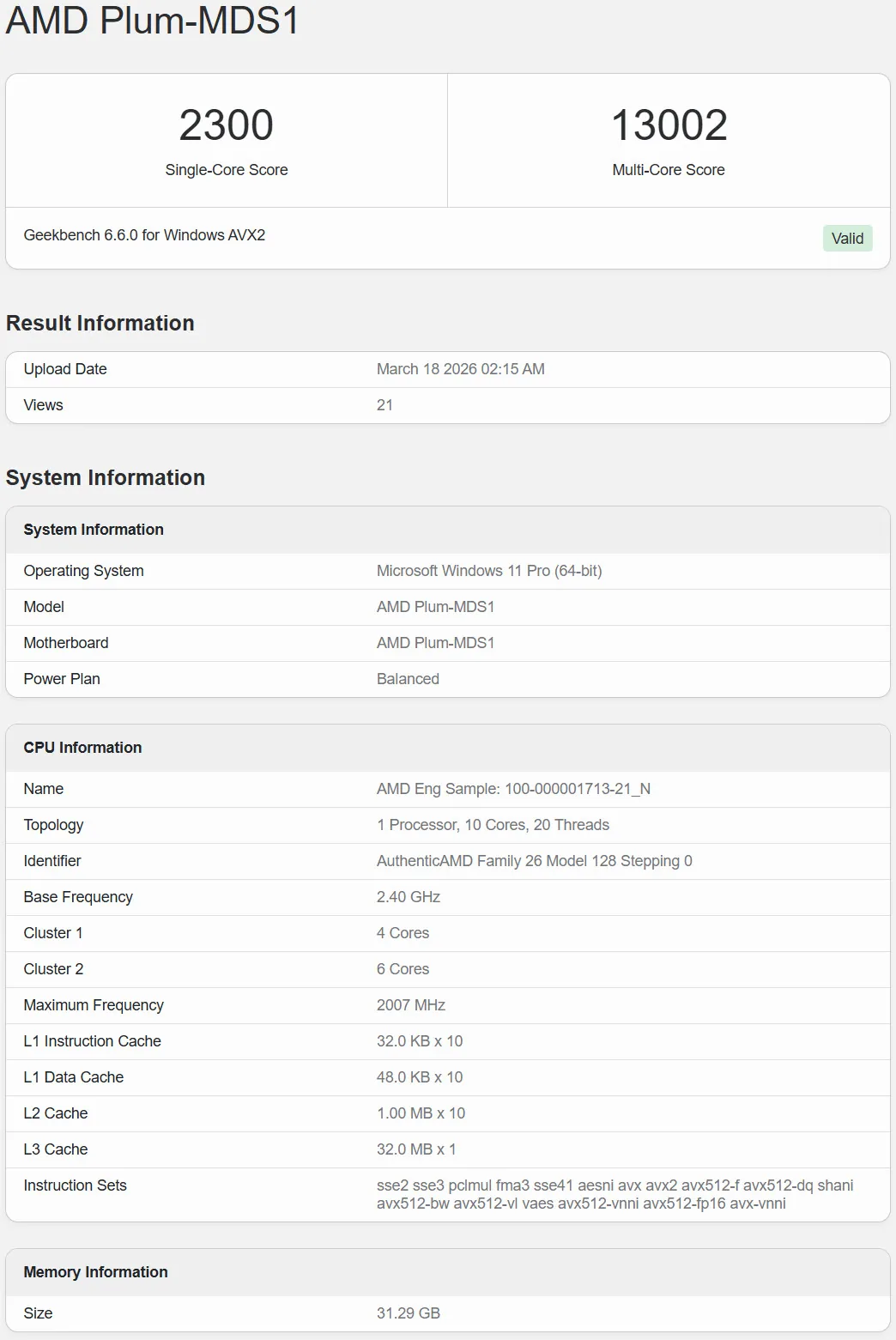
The earliest sightings of the architecture surfaced in March 2026, when an engineering sample running on an internal Plum-MDS1 evaluation board appeared in the Geekbench database with a modest 2.0 GHz clock speed. That test was spotted by Benchleaks and covered by Hassan Mujtaba at Wccftech. The initial 10-core sample posted a single-core score of 2,300 and a multi-core score of 13,002 [6]. By July, newer test submissions identified as sample 100-000001713-33_N began showing much higher numbers on the same platform as engineers continued evaluating AMD Medusa Point silicon across early firmware revisions. In those runs, the processor reached 3,174 points in single-threaded testing and 15,092 points in multi-threaded workloads, topping existing flagship laptop chips even before reaching final retail tuning. Hassam Nasir at Tom’s Hardware noted that “Medusa Point looks to be promising” given how early silicon outpaced current hardware [2].
Performance climbed again in late July when Geekbench logs showed the same 10-core sample scoring 3,329 points in single-core and 16,555 points in multi-core testing. Boost clocks reached 5.37 GHz. The single-core score matched AMD’s desktop Ryzen 9 9900X [3].
Fresh listings from November 2026 revealed broader testing on prototype Lenovo hardware under system codes such as LENOVO 22ETPF6DTA and LENOVO 22EUFVT027, as spotted by HXL and Olrak. In Geekbench 7, sample 100-000001713-32_Y scored 3,100 points in single-core testing. Multi-core output reached 18,313 points on the Lenovo system. While earlier silicon had matched desktop parts in short bursts, these Lenovo runs proved that laptop makers were actively putting Zen 6 through prolonged validation runs across varying power profiles [1].

Configurations for AMD Medusa Point Chips
The leaked listings outline a flexible lineup built around a hybrid mix of standard Zen 6 cores and smaller Zen 6c cores, defining the AMD Medusa Point architecture for mainstream laptops. At the top of the mainstream tier sits a 10-core, 20-thread processor that combines four Zen 6 performance cores with six Zen 6c compact cores. Smaller models also appeared in testing, including an 8-core part pairing two Zen 6 cores with six Zen 6c cores, and a 6-core variant with a single Zen 6 core and five Zen 6c cores [1]. AMD chose this split design to balance computing power with battery life in thin notebooks. Crmaris at Hardware Busters noted that the split layout helps thin laptops manage thermal limits without throttling main performance cores [5].
System information logs reveal distinct family identifiers for the different silicon revisions. Medusa Point 1 processors carry the AuthenticAMD Family 26 Model 129 identifier, whereas Medusa Point 2 and 3 chips use Model 224. Prototype Lenovo laptops paired the 10-core chip with 64 GB of DDR5-5200 memory [1].
Leak data assigns the silicon a 32-megabyte level-three pool alongside 10 megabytes of second-level storage, though Hassam Nasir at Tom’s Hardware cautioned that early benchmarks often misread tertiary cache numbers on pre-release silicon [2]. Geekbench entries also flagged native support for AVX-VNNI FP16 instructions within the Zen 6 instruction set [4]. Native FP16 execution allows Zen 6 CPU execution units to run low-precision machine learning inference and media processing directly on the core, bypassing the delay of offloading small calculations to separate accelerators [5]. The feature aids Windows 11 on-device AI tasks [4].


Comparisons with Current Ryzen Processors
Side-by-side benchmark runs demonstrate how AMD Medusa Point processors outpace predecessor architectures across diverse workloads. In Geekbench 7 single-core testing, the 10-core engineering sample scored 28% higher than the 16-core Ryzen AI Max+ 395 and 32% ahead of the 12-core Ryzen AI 9 HX 370 running in retail notebooks. In multi-threaded tests, the same sample outpaced the Ryzen AI 9 HX 370 by 21.5%, despite carrying two fewer hardware cores [1]. Hilbert Hagedoorn at Guru3D reported that the 10-core part also closed in on AMD’s flagship Strix Halo silicon [4]. The lead stems from generational improvements in execution efficiency, proving that Zen 6 doesn’t rely solely on raw clock frequency to gain ground [2].
Could early clock speed reports obscure the true performance of the architecture? The July Plum-MDS1 run reached 3,174 points at 2.0 GHz, beating the Ryzen AI 9 365 by roughly 29% in single-threaded tasks [4]. Qualcomm’s 18-core Snapdragon X2 Elite led mobile single-core standings with 3,573 points, leaving the 10-core AMD sample only 7% behind [3].
Desktop comparisons further illustrate the strength of the mobile engineering sample. With a single-core score of 3,329 points, the mobile processor ran neck-and-neck with AMD’s desktop Ryzen 9 9900X and Ryzen 7 9800X3D, which both scored around 3,333 points in the same benchmark. It also surpassed Intel’s Core i9-14900KS and Core Ultra 9 285K desktop processors in single-threaded output. In multi-core testing, the engineering sample reached 16,555 points, approaching the desktop Ryzen 5 9600X [3].

Integrated RDNA 4m Graphics Scores
In addition to general CPU compute results, the November leak provided the first benchmark numbers for AMD’s integrated graphics architecture, listed under the board code gfx1170. Hassan Mujtaba reported that the graphics core ran on the 10-core engineering sample and features four RDNA 4m compute units. This design combines architectural blocks from both RDNA 3.5 and RDNA 4 into an updated graphics subsystem tailored for compact mobile systems. In the Geekbench OpenCL test, the graphics unit delivered a score of 22,249 points, showing strong rendering capability for an entry-level mobile configuration. The graphics core carried four compute units [1].
The 22,249 OpenCL tally places the new graphics core well above older entry-level mobile Radeon GPUs. The Radeon 840M, carrying four RDNA 3.5 compute units, scored 12,019 points. AMD’s newer RDNA 4m sample landed ahead of the Radeon 860M at 20,642 points, trailing only the Radeon 880M at 26,814 points [1].
Hardware reports from Hilbert Hagedoorn at Guru3D indicate that AMD might also prepare integrated graphics configurations with up to eight compute units on select Medusa Point models. Doubling the compute unit count would let mainstream thin laptops handle casual gaming and media editing without requiring add-in graphics cards [4]. While AMD’s top-end Strix Halo chips continue to serve high-power creator notebooks, Medusa Point’s integrated graphics focus on power efficiency and compact die area. Early tests show that the new design extracts more work from every compute block than previous architectures [1].

Market Arrival for AMD Medusa Point Laptops
Current industry roadmaps indicate that AMD will introduce its Medusa Point family at CES in January 2027, positioning the silicon as the mainstream Ryzen AI 500 mobile lineup to succeed the existing Ryzen AI 400 series in retail laptops [1]. Motherboard listings associate the silicon with AMD’s FP10 BGA socket [5]. Operating between 28W and 45W thermal envelopes lets PC makers install the hardware in portable chassis without requiring bulky cooling systems or loud fans [6].
AMD’s product launch schedule aligns Medusa Point with broader updates across the company’s computing portfolio [3]. Desktop Zen 6 processors and server hardware will roll out during the same broader generational transition [5]. The company has already demonstrated its high-end computing plans with server silicon, as explored in recent coverage of AMD EPYC Venice server processors and their 256-core designs. In the mobile market, Medusa Point will compete head-to-head with Intel’s upcoming Panther Lake platform, while AMD’s Gator Range chips will target top-tier gaming laptops [3]. Crmaris at Hardware Busters noted that mobile APUs often follow desktop and server releases, making Medusa Point an important piece in AMD’s complete Zen 6 rollout [5].
Because these benchmark entries represent pre-release engineering samples, final retail specifications could still shift [2]. Clock speeds, power limits, and BIOS firmware undergo extensive tuning during the months leading up to mass production [4]. Even so, multiple benchmark submissions confirm that Zen 6 silicon is advancing on schedule [3]. For consumers planning a laptop upgrade in 2027, Medusa Point promises noticeable leaps in responsiveness [1].
- ONLINE NEWS Mujtaba, H. (2026, November 7). AMD Medusa 10, 8, 6 Core APU & RDNA 4m “GFX1170” Benchmarks Leak With Zen 6 Delivering Strong Single & Multi-Core Performance. Wccftech. [Article Link]
- ONLINE NEWS Nasir, H. (2026, July 9). AMD’s upcoming Zen 6 Medusa Point 10-core APU pops up on Geekbench — chip is faster than Ryzen AI 9 HX 370 & even Ryzen AI Max+ 395. Tom’s Hardware. [Article Link]
- ONLINE NEWS Hagedoorn, H. (2026, July 20). AMD Zen 6 Medusa Point APU Posts Fastest x86 Mobile Geekbench Single-Core Score Yet. Guru3D. [Article Link]
- ONLINE NEWS Hagedoorn, H. (2026, July 9). AMD 10-Core Zen 6 Medusa Point APU Appears Again in Geekbench with Higher Performance. Guru3D. [Article Link]
- ONLINE NEWS Crmaris. (2026, July 13). AMD’s 10-core Zen 6 “Medusa Point” turns up in Geekbench — beating today’s fastest mobile Ryzen. Hardware Busters. [Article Link]
- ONLINE NEWS Mujtaba, H. (2026, March 18). AMD Medusa Point Leak Shows 10 “Zen 6” Cores At 2 GHz Faster Than 10 “Zen 5” Cores at 5 GHz. Wccftech. [Article Link]


