






Can scientists alter atomic flaws in a crystal without ruining the fragile quantum bits already sitting inside? Solid-state physics often treats defects in carbon lattices as a blended mixture where any thermal change disturbs every center at once. A team led by Jiaxin Ye at North Carolina Central University showed that a nanosecond uv laser pulse can modify selected carbon flaws while leaving background nitrogen-vacancy centers intact [1].
- What Are UV Lasers Used for in Quantum Materials?
- How Do UV Laser Pulses Work on Crystal Defects?
- Preserving Nitrogen-Vacancy Qubits During Optical Processing
- Engineering Selected Color Centers With UV Laser Pulses
- Spectroscopic Mapping After Ultraviolet Laser Pulses
- The Unresolved Atomic Pathways of Diamond Modification
What Are UV Lasers Used for in Quantum Materials?
UV lasers are used to excite electronic states and modify specific crystal defects without bulk heating of the substrate. In diamond engineering, short optical pulses deliver focused energy to tight spots so the team can create or adjust optical color centers for computing and nanoscale field sensing, triggering local lattice shifts while preserving deeper structures that would break down under furnace annealing [1]. Optical control matters for developing solid-state quantum hardware.
Pure diamond consists of carbon atoms locked into a rigid tetrahedral crystal lattice where any missing atom, misplaced atom, or foreign element introduces an atomic flaw that alters how the crystal absorbs and emits light [2]. Some of these atomic imperfections act as quantum systems with clear electron spin states. The nitrogen-vacancy center, pairing a single nitrogen atom with an empty lattice vacancy, provides a stable spin qubit that operates at room temperature for magnetometry and electric field sensing. Building practical quantum devices requires tuning neighboring defect populations without degrading those sensitive native qubits.
Past methods often relied on ion implantation followed by thermal annealing at extreme temperatures, but high furnace heat tends to alter all defects across the sample indiscriminately rather than targeting specific color centers. In contrast, scientists studying optical data capacity and diffraction limits in diamonds have explored focused light to control color centers in small, micrometer-scale volumes [1]. The central experimental question was whether optical pulses could alter carbon defects while leaving native NV centers unchanged.

How Do UV Laser Pulses Work on Crystal Defects?
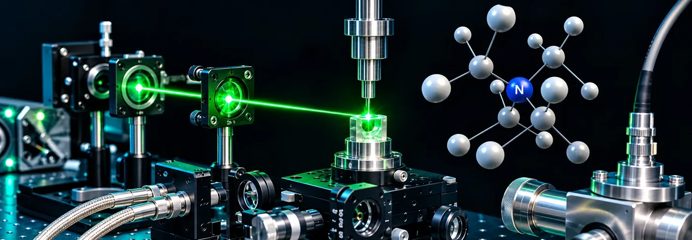
Short uv laser pulses work on crystal defects by delivering energetic ultraviolet photons that drive single-photon electronic transitions and rearrange neighboring carbon atoms without melting or heating the surrounding diamond lattice. In a study published in Diamond and Related Materials, the team irradiated focused regions of synthetic diamond using ultraviolet light at a wavelength of 266 nanometers, delivering pulses lasting only six nanoseconds [1]. Confining the beam energy in time and space enabled local atomic modifications without heating the whole crystal.
The experiments used single-crystal diamond grown by chemical vapor deposition (CVD), a synthesis method for producing high-purity substrates with minimal nitrogen impurities and uniform crystal transparency throughout the entire sample thickness. Before turning on the laser, visiting graduate student Emmanuel Ediri Umukoro and his colleagues mapped the pristine diamond using confocal photoluminescence, verifying optical transparency with UV-visible absorption spectra and tracking impurity levels with Fourier-transform infrared spectroscopy [3]. The pristine sample had low nitrogen content. Setting this baseline was necessary because scientists could not otherwise distinguish defect signatures created by laser pulses from those already present in the starting chemical vapor deposition crystal.
The team tested laser fluences—the optical energy delivered per unit area—spanning between 2.2 and 8.6 joules per square centimeter across focused regions of the diamond crystal. Because 266-nanometer photons fall below the fundamental bandgap of diamond, they interact with local electronic states tied to defects rather than triggering bulk electron excitation across the full valence-to-conduction bandgap. The measured signal intensity scaled linearly with laser fluence, exhibiting a power-law exponent of 1.10 ± 0.16 that is consistent with a single-photon excitation process [2]. Single photons drove the observed atomic shifts.
Preserving Nitrogen-Vacancy Qubits During Optical Processing
The central finding of the experiment was that preexisting nitrogen-vacancy centers survived the laser treatment with their optical properties and zero-phonon emission intensities largely unchanged compared to unexposed regions. When scientists examined the irradiated spots, the characteristic photoluminescence signals from native NV centers showed negligible variation, proving that nanosecond pulses can alter nearby carbon defects without destroying existing qubits [1]. This resilience enables selective modification around an operating sensor.
Nitrogen-vacancy centers are among the most studied color centers in physics because their spin states can be initialized, manipulated, and read out optically at room temperature for high-sensitivity magnetic and electric field metrology. Similar measurement precision drives research into laboratory trials of thorium nuclear clocks, where quantum-level transitions unlock new measurement thresholds across fundamental physics and high-precision frequency standards [1]. The stability of the native NV population proved that selective modification in diamond is achievable.
Senior study authors pointed out that NV centers remained stable under the exact laser fluences that produced new optical features, showing that optical excitation can differentiate between defect families inside diamond. “We show that these nanosecond laser pulses can selectively engineer the 563-nm center, a self-interstitial-related defect, without affecting the background nitrogen-vacancy (NV) center,” the authors said [1]. The laser altered carbon atoms without disturbing nitrogen-vacancy pairs.


Engineering Selected Color Centers With UV Laser Pulses
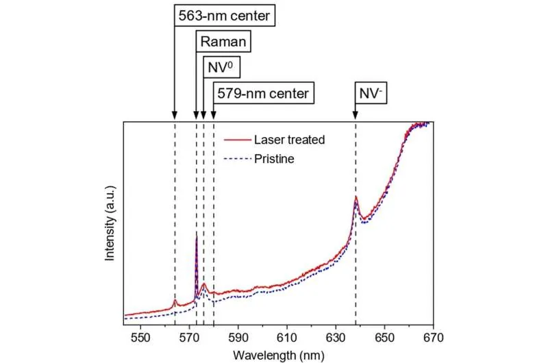
Following laser irradiation, confocal photoluminescence scans revealed a new emission peak at 563 nanometers that was absent in the pristine diamond, alongside a secondary emission feature near 579 nanometers [1]. Earlier crystallographic studies linked both optical signatures to carbon self-interstitials, in which carbon atoms are knocked out of regular lattice sites into interstitial positions during irradiation [2]. The laser produced defined point defects with sharp emissions.
Continued exposure revealed that the 563-nanometer emission did not climb indefinitely as the crystal absorbed more laser pulses, but instead reached a maximum signal intensity before declining under prolonged irradiation [3]. This non-monotonic response shows that optical pulses can both generate and transform defect structures over time. “Our study demonstrates that nanosecond laser pulses can achieve selective engineering of point defects in diamond and is promising for deterministic control of diamond color centers for quantum applications,” the researchers stated [2].
Lead author Jiaxin Ye and co-author Emmanuel Ediri Umukoro, writing in a report shared through Science X Dialog, clarified that these new centers are not yet demonstrated quantum qubits. The practical value of the experiment lies in manipulating one defect population while leaving quantum sensors untouched, using the 563-nanometer emission as a testbed for studying defect dynamics [3]. Tracking this peak reveals limits of lattice modification.
Spectroscopic Mapping After Ultraviolet Laser Pulses
High-resolution two-dimensional photoluminescence mapping allowed the research team to track zero-phonon line integrated intensities across the treated areas, confirming that the 563-nanometer emission matched the precise spatial coordinates of the laser spot. Outside those exposed spots, the diamond retained its original, pristine spectroscopic signature, proving that defect generation occurs only where the ultraviolet beam delivers sufficient fluence without affecting surrounding material [1]. Unexposed regions of the crystal remained fully unchanged.
Optical tests at room temperature provided clear comparisons between treated and untreated zones, showing that pristine CVD diamond exhibited minimal background luminescence due to its low nitrogen content and high crystal purity. Laser exposure introduced the sharp 563-nanometer zero-phonon line without broadening preexisting nitrogen-vacancy lines, an important outcome because maintaining narrow spectral linewidths is essential for high-fidelity optical readout in quantum sensing applications [1]. Surrounding carbon bonds remained structurally stable during optical exposure.
Umukoro, a graduate student at North Carolina Central University and a visiting graduate student in Electrical and Computer Engineering at Duke University, noted that local optical excitation avoids destructive furnace heating. The research team verified that optical properties changed without causing diamond surface ablation or graphitization, preserving the transparent sp3 carbon bonding network that optical sensors require for long-term operational stability [3]. The crystal retained its transparent diamond bonding network.
The Unresolved Atomic Pathways of Diamond Modification
The exact microscopic pathway that drives these defect shifts remains an unresolved scientific question in diamond physics. Because 266-nanometer photons have less energy than the fundamental diamond bandgap, the laser cannot excite electrons across the valence-to-conduction gap through direct single-photon absorption without local intermediate states already present in the lattice. The authors suggest that incoming light couples to electronic levels already bound to flaws, transferring pulse energy into the nearby crystal mesh to move carbon atoms around [1].
Trapped charge carriers and excitons may also play an important role in driving these atomic shifts under nanosecond pulses, but current optical data cannot pinpoint the exact geometric layout of the centers. Many distinct arrangements of carbon self-interstitials produce overlapping optical lines, meaning that until theoretical modeling resolves the microscopic structure, scientists cannot predict every atomic transition on a deterministic basis [1]. The process shows clear optical control over defect populations.
The current study does not show a functional quantum device or prove deterministic defect creation on demand, but it sets an experimental framework showing that diamond defects are not inseparable. Future experiments will focus on linking laser pulse duration and fluence to specific defect outcomes so scientists can tailor diamond substrates for quantum sensors, optical memories, and distributed quantum communication networks [2]. Carefully controlled laser parameters may unlock custom quantum materials.
- ACADEMIC JOURNAL Ye, J., Umukoro, E. E., Serpa, R. B., Amsden, J. J., Brown, A. S., Glass, J. T., Flanigan, P., Vlahovic, B., Oni, O., Wu, M., & Parker, C. B. (2026). Selective engineering of color centers in diamond using ultraviolet nanosecond laser pulses. Diamond and Related Materials, 169, 114126. [Article Link]
- ONLINE NEWS Brahambhatt, R. (2026, October 11). Laser pulse creates defects in diamond but spares quantum center. Interesting Engineering. [Article Link]
- ONLINE NEWS Umukoro, E. E. (2026, October 10). Ultraviolet laser pulses engineer diamond defects selectively, leaving quantum qubits intact. Phys.org. [Article Link]
APA 7: TWs Editor. (2026, October 12). Diamond Defects Shift Under UV Laser Pulses Without Qubit Loss. PerEXP Teamworks. https://perexpteamworks.com/en/uv-laser-pulse-diamond-defects/


