





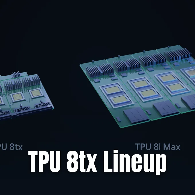
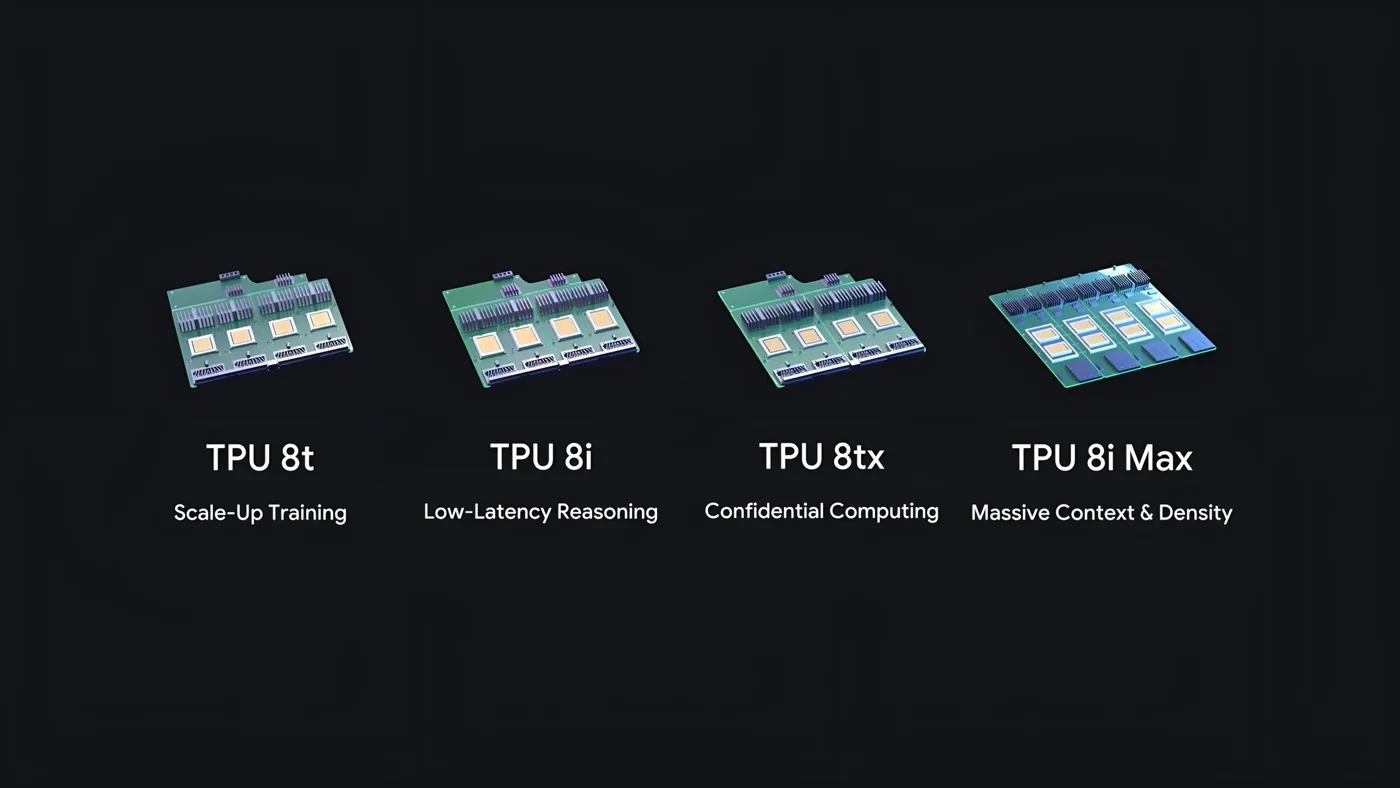
Google unveiled two eighth-generation server systems in its custom artificial intelligence silicon family on November 9, 2026 [3]. The company added the TPU 8tx for confidential inference, and it packaged two TPU 8i processors together in the TPU 8i Max to handle massive context windows [1]. Both offerings expand upon the TPU 8t and TPU 8i accelerators that Google introduced at Google Cloud Next in April [3]. Instead of designing new silicon dies from scratch, Google modified packaging, host CPUs, and networking around existing eighth-generation chips to power agentic AI workloads [2].
Architecture of the TPU 8tx
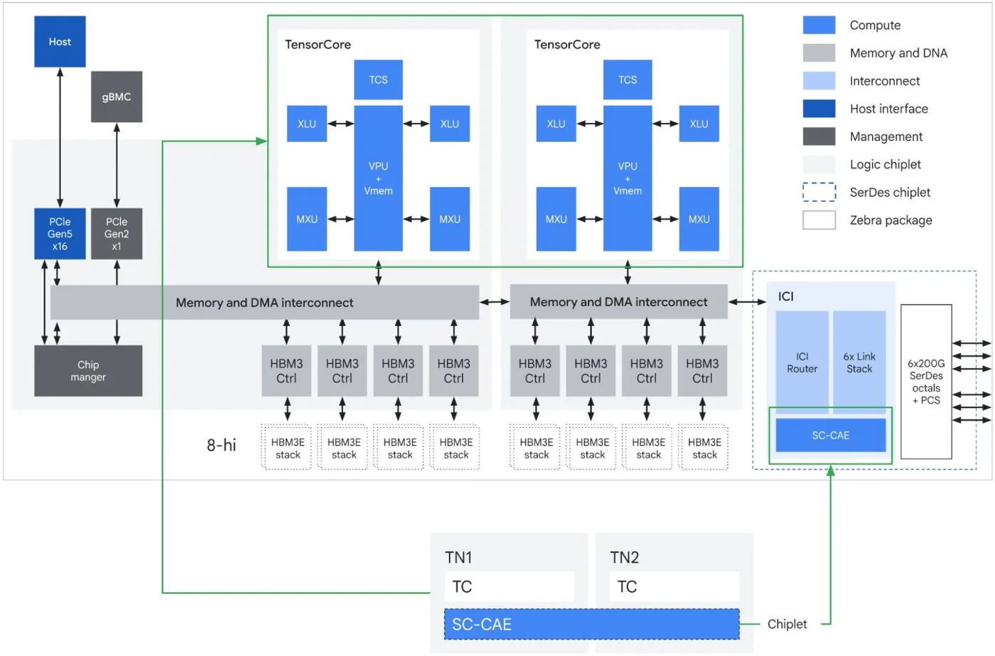
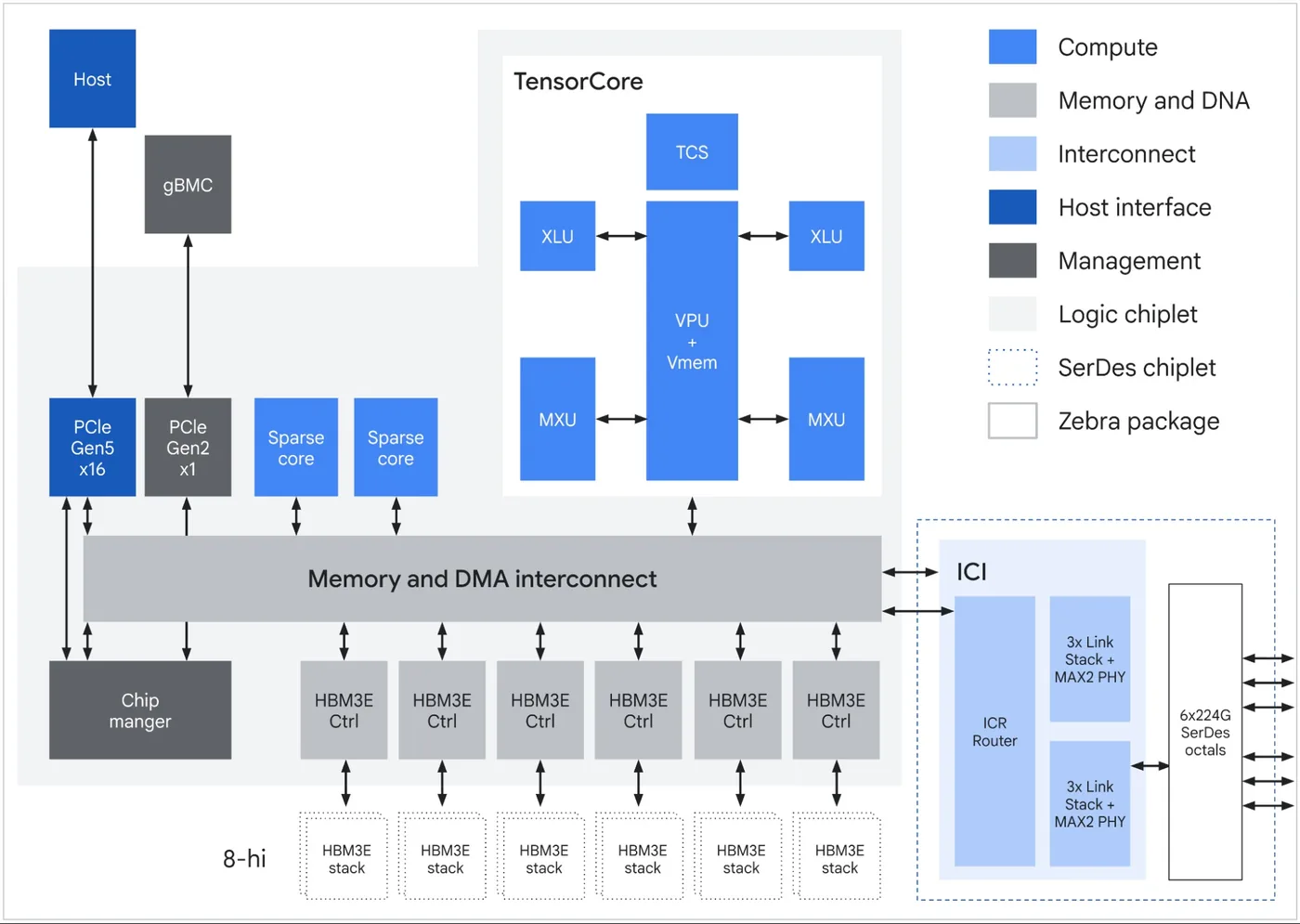
The TPU 8tx uses the logic chiplet from Google’s TPU 8t training processor. Rohail Saleem of Wccftech noted that this chiplet sits inside Google’s Zebra package, which houses a central logic die, an off-chip SerDes component with 6x224G SerDes octals, and six 8-hi HBM3E memory stacks. Each TensorCore pairs a central Vector Processing Unit with dedicated Vector Memory (Vmem). It connects directly to two Matrix Multiply Units (MXUs) and two eXtended Logic Units (XLUs), where native 4-bit floating point (FP4) execution yields 12.6 PFLOPS of processing power per chip while overlapping vector operations with matrix multiplication. Two sparse cores also offload irregular memory lookups [1].
Google swapped out Arm-based Axion processors for custom fifth-generation AMD EPYC CPUs [1]. While data center operators track how AMD EPYC processors handle high-density server workloads, Google chose these specific x86 hosts to run secure enclaves that protect customer datasets and model weights directly in hardware throughout active inference. Standard servers decode private data before compute units can read it [3].
Google also changed networking on the TPU 8tx [1]. The system adopts the Boardfly interconnect topology developed for the TPU 8i, and Google said this design cuts latency by up to half compared to standard TPU 8t servers without creating security overhead. Engineering teams can fine-tune private models, distill networks, and run reinforcement learning inside a single protected rack [2].
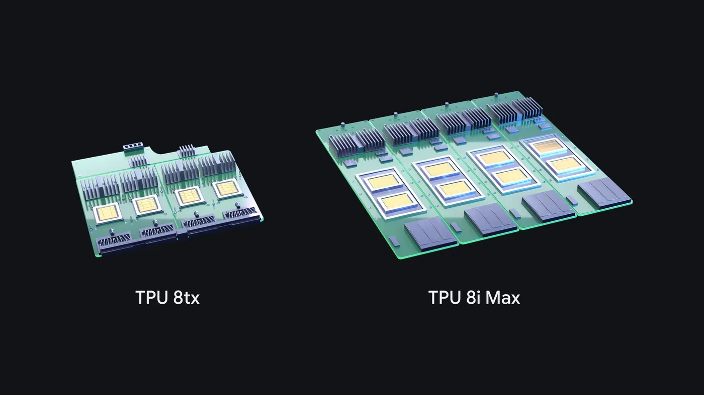
Dual-Chip Design of TPU 8i Max
Google built the TPU 8i Max to solve memory wall bottlenecks [1]. Instead of manufacturing an oversized monolithic die, Google joined two distinct TPU 8i chips on one package, combining four TensorCores, sixteen HBM3E memory stacks, and 768 MB of SRAM into standard rack enclosures [2]. Each individual logic die contains two memory interconnect blocks. These interconnect blocks link compute elements to four HBM3 controllers, enabling 6x200G SerDes octals to route off-chip traffic across custom network topologies [1].
The dual-chip package delivers an estimated peak performance of 20.2 PFLOPS in FP4 precision and roughly 17.2 TB/s of memory bandwidth. Google also pools 768 MB of on-chip SRAM directly on the module to store active key-value (KV) caches [2]. Google hasn’t published absolute HBM capacity for the combined unit, but each individual 8i chip carries 288 GB of HBM3e running at 8.6 TB/s [1].
On-chip SRAM storage lets the processor read vital parameter layers without querying external host memory [1]. Cloud facilities can double their available compute density without expanding floor space or installing taller racks [2]. Kyt Dotson of SiliconANGLE reported that this physical density helps data centers lower floor space and electricity requirements per watt [3].

Context Window Demands for AI Agents
Modern AI workloads demand vast memory [2]. As developers transition from basic prompt-response exchanges to autonomous agents that inspect entire codebases, context windows must hold complete repository histories, hours of video, or hundreds of documents in active working storage. A model references this working space while answering complex user queries [3].
Google’s Gemini frontier model supports an industry standard 1 million tokens, which equals about 750,000 words or 1,500 pages of text. Smaller open-source models often run with narrower windows between 128,000 and 256,000 tokens, but maintaining rapid responses still puts heavy pressure on hardware. A wider context window forces processors to swap data in and out of working storage constantly. When an accelerator lacks fast on-die SRAM, the model spends extra cycles waiting for memory transfers, and that delay increases the power needed to “think” through complex prompts [3]. By providing 768 MB of SRAM alongside 17.2 TB/s of bandwidth, the TPU 8i Max keeps active tokens accessible to compute cores during multi-step reasoning tasks [2].
With high memory bandwidth, the TPU 8i Max lets AI agents inspect long documents without stalling. Digital assistants that generate code, check legal compliance, or summarize research papers can keep full project histories in active memory [2]. These hardware additions give data centers practical tools to run multi-agent workflows without splitting jobs across oversized server clusters [3].
Software Tools Supporting the TPU 8tx
Google introduced several software updates to help engineers write code for the TPU 8tx and eighth-generation TPU systems. The company recently open-sourced TorchTPU, so engineers can run PyTorch and Hugging Face models natively on TPU silicon without tedious manual rewrites. Serving frameworks including vLLM and SGLang also gained official TPU execution backends. Google released an early preview of its TPU agent suite, which connects directly to Claude Code, Cursor, and Antigravity to help developers onboard and tune low-level computing kernels [2].
Google built an open-source C++ library named TPU Sync. The software tiers key-value cache data across high-bandwidth memory, host system DRAM, and secondary storage. In benchmarks running the Qwen3 235B model, TPU Sync cut median cache transfer latency from several seconds to 230 ms, and time to first token fell 60% on 235B and 90% on the 480B model under low concurrency. These benchmark tests ran on earlier Ironwood TPU v7x hardware instead of new v8 systems. Off-chip cache tiering during pauses keeps active sessions ready for follow-up prompts [2].
Orchestration tools also received updates for agent traffic. Google made both Cloud Pathways and Google Kubernetes Engine dynamic slicing generally available, which speeds up fault recovery by up to 4.5 times and cuts job startup delays up to 5 times. Google also plans to preview an Agent Compute Engine to pause idle sessions and shift working memory off-chip [2].
Data Center Deployments and Hardware Comparisons
Google introduced its latest hardware as cloud providers expand custom silicon programs to challenge Nvidia in data centers [1]. Nvidia plans to start volume production of its dual-die Rubin GPU in the second half of 2026, targeting 50 PFLOPS of FP4 performance with 288 GB of HBM4 memory and Nvidia Vera host CPUs. Microsoft unveiled its TSMC 3nm Maia 200 chip in January 2026, delivering over 10 PFLOPS with 216 GB of HBM3e and 272 MB of SRAM. AWS announced Trainium3 in December 2025, offering 2.52 PFLOPS in FP8 precision paired with 144 GB of memory [2]. Each cloud provider adapts physical server hardware to balance software demands and operating costs [1].
Competitors mostly target general cloud computing capacity, but Google tailored these two eighth-generation systems around specific architectural bottlenecks [1]. The dual-chip TPU 8i Max attacks the memory wall by providing an estimated 17.2 TB/s of bandwidth, which gives agents enough memory speed to process million-token contexts without delay [2]. At the same time, the TPU 8tx addresses regulatory compliance by locking weights and live inputs inside hardware enclaves managed by custom AMD host processors [1]. Regulated teams in healthcare, finance, and government can fine-tune private models on confidential data without moving records between unencrypted systems [3]. These design choices prioritize memory density and data security over single-chip compute records [2].
Google hasn’t published official prices or benchmark results. According to reporting from Bloomberg via Quartz, initial availability for both the TPU 8tx and the TPU 8i Max is planned for 2027. Until volume shipments begin, cloud customers will continue running existing TPU 8t training clusters and TPU 8i inference servers while evaluating early preview software such as TorchTPU and TPU Sync [2].
- ONLINE NEWS Saleem, R. (2026, November 9). Google Pairs Its New TPU 8tx With Custom AMD EPYC CPU Hosts, While The TPU 8i Max Combines Two TPU 8i Chips In A Single Package To Offer Phenomenal Compute And Memory Density. Wccftech. [Article Link]
- ONLINE NEWS MarkTechPost. (2026, November 9). Google Unveils TPU 8i Max and TPU 8tx: A Dual-Chip TPU and a Confidential TPU. MarkTechPost. [Article Link]
- ONLINE NEWS Dotson, K. (2026, November 9). Google advances agentic AI custom silicon expanding TPU family with 8tx and 8i Max. SiliconANGLE. [Article Link]


