





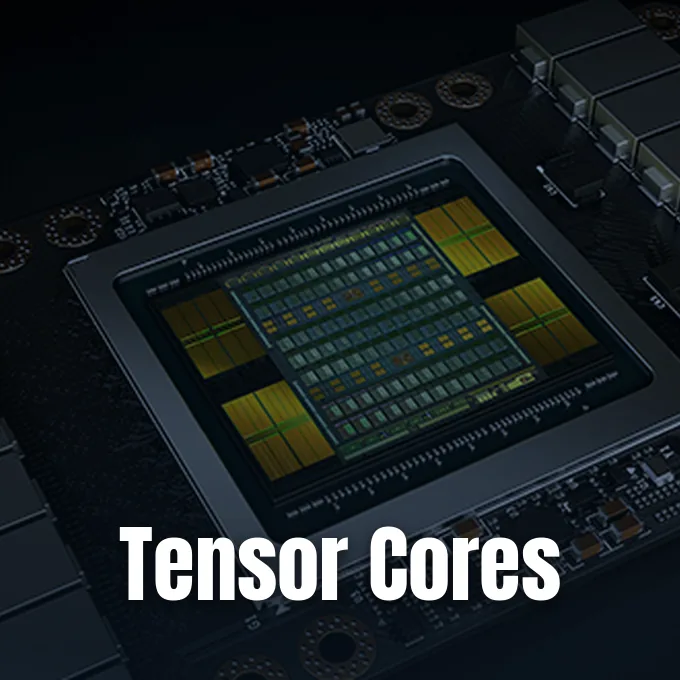
Nvidia introduced tensor cores to accelerate matrix math inside graphics processors, shifting how hardware handles artificial intelligence workloads. AI relies on matrix math. Before their arrival on data center silicon, standard graphics processors calculated deep learning algorithms by breaking large matrices into individual scalar floating-point equations inside general-purpose streaming units [4]. Modern deep learning models rely on multiplying multidimensional arrays of numbers, known as tensors, billions of times during training and inference passes [3]. Tensor cores execute these mathematical steps in hardware by processing small matrix blocks in a single clock cycle [4].
What Are Tensor Cores?
Graphics processing units traditionally relied on CUDA cores to run basic instructions. A standard CUDA core handles one math step per clock tick, such as an addition or a multiplication on single scalar values. In contrast, an Nvidia Tensor Core runs as a custom execution unit built specifically for matrix multiply-accumulate work, grouping calculations into dense numerical blocks so graphics hardware achieves higher compute density while reducing electrical power draw [3, 4].
At the silicon level, early designs focused on handling small math tiles. The first-generation design inside the Volta microarchitecture takes two 4×4 matrices of 16-bit floating-point numbers, multiplies them together, and adds a third 4×4 matrix to the product. Engineers write this step as D = A * B + C. The accumulation step keeps numbers stable by adding intermediate products into a 32-bit floating-point accumulator, which stops rounding errors from compounding across deep layers. How does silicon maintain speed when network models scale into billions of parameters? It bypasses register bottlenecks by running sixteen dot products in one step, letting an Nvidia streaming multiprocessor calculate dozens of matrix numbers at once without stalling instruction queues [1, 4].
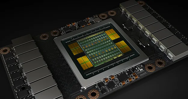
Standard shaders in processors like the Nvidia Volta GV100 and Nvidia Quadro GV100 still handle rasterization, geometry transforms, texture filters, and general program flow while matrix circuits remain idle. Inside each streaming multiprocessor, specialized tensor units sit next to integer and floating-point pipelines, activating only when software issues matrix multiply-accumulate commands [1, 4]. When applications call linear algebra routines, the GPU steers matrix tiles into these paths to run fast without slowing down basic graphics work [1].
Matrix Multiply-Accumulate Operations
Neural networks spend most of their execution time computing matrix multiplication across deep learning layers. Fully connected layers, self-attention projections in transformer models, and convolutional filters all map to generalized matrix multiplication, known as GEMM. In these steps, input data multiplies by learned weight values to create outputs for the next network layer. Because large models hold billions of parameters, calculating these steps with scalar commands creates massive register traffic [3].
Multiply-accumulate hardware removes this bottleneck by running matrix steps as atomic commands. In a single run, the unit loads a tile from matrix A and a tile from matrix B, finds the inner products, and adds the accumulator matrix C [4]. The fused step finishes in fewer clock ticks than separate multiply and add steps while avoiding intermediate rounding steps [5].
Software tuning helps keep matrix units fed with data during intensive training tasks. In a 2026 performance study published on Zenodo from CERN, researcher S. T. Ejaz tested matrix multiplication on an Nvidia Tesla T4 GPU by benchmarking custom CUDA code written with the Warp Matrix Multiply and Accumulate API against the official Nvidia cuBLAS library. The code used 16-bit inputs with 32-bit accumulation and reached 63% to 67% of cuBLAS speed. Ejaz noted that because the Tesla T4 card lacks hardware asynchronous copy features, double buffering shared memory gave no speed gain over a single buffer design. This test showed that compute circuits need matching memory copy paths to stay fully busy [7, 9].
Evolution From Volta to Blackwell
Nvidia launched its first matrix hardware in 2017 with the Volta microarchitecture, built on a TSMC 12 nm FinFET process with 21.1 billion transistors and named after physicist Alessandro Volta. Designed as the primary accelerator for the Nvidia DGX-1 server, the enterprise Nvidia Tesla V100 card included 640 Tensor Cores delivering 125 teraflops of deep learning speed, representing a fivefold gain over previous Pascal chips [1, 4]. High Bandwidth Memory 2 supplied 900 gigabytes per second of bandwidth while NVLink 2.0 connected host processors with 25 gigabits per second per lane. Volta also ran in the Titan V and Quadro GV100, and paired with IBM POWER9 processors in the Summit and Sierra supercomputers [4].
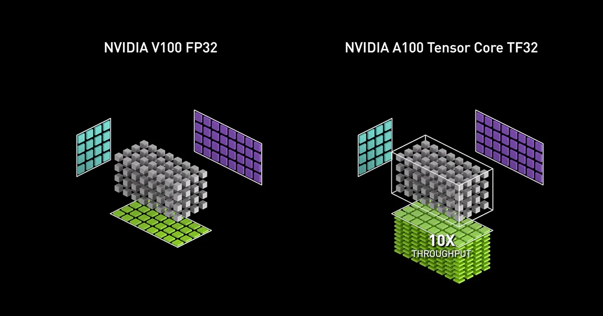
The Nvidia Ampere generation arrived in 2020, dropping the Tesla moniker to establish the A100 Tensor Core GPU as its flagship enterprise platform [3]. Described by Nvidia engineers J. Choquette, W. Gandhi, O. Giroux, N. Stam, and R. Krashinsky in IEEE Micro, the Nvidia A100 added third-generation matrix units with support for TensorFloat-32, Bfloat16, and 64-bit floating-point math [7]. The Nvidia A100 delivered 19.5 teraflops of FP64 matrix speed and 312 teraflops of FP32 tensor throughput. Two years later, the Nvidia Hopper architecture brought the Nvidia H100 and Nvidia H200, introducing a Transformer Engine that pushed FP8 tensor math to 4 petaflops [3].
The Nvidia Blackwell microarchitecture advanced this line in 2025 with fifth-generation units built around narrow numeric formats. The Nvidia B200 and Nvidia Blackwell Ultra B300 chips carry a second-generation Transformer Engine supporting 4-bit floating-point precision, named NVFP4 and FP4 [2]. By shifting silicon space away from heavy FP64 math to lower bits, the Nvidia B300 hits 14 petaflops of dense FP4 tensor speed and 18 petaflops of sparse tensor throughput [3].
How Tensor Cores Handle Mixed Precision
Mixed-precision arithmetic forms the foundation of hardware matrix units. In classic high-performance computing, simulations use 64-bit double precision or 32-bit single precision to stop rounding drift. Neural networks tolerate lower bit widths because training tunes statistical weights rather than finding exact proofs. Low bit sizes save memory space. Storing values in 16-bit or 8-bit formats cuts memory traffic by half, freeing cache space and lowering power draw [1, 3].
Multiplying in reduced bit sizes while adding into full precision keeps training stable across complex network models. When tensor units run math, they multiply inputs stored in formats like FP16 or Bfloat16 and accumulate those products into 32-bit floating-point registers [4]. The Nvidia Ampere generation added TensorFloat-32, a mode using the 8-bit exponent of FP32 for range and the 10-bit mantissa of FP16 for speed, letting developers speed up FP32 training without altering code. This format helps engineering teams gain fast matrix throughput across existing software without changing model parameters [7, 8].
Researchers M. Fasi, N. J. Higham, M. Mikaitis, and S. Pranesh studied this floating-point behavior in a 2021 paper published in PeerJ Computer Science. Testing the Nvidia Tesla V100, Nvidia Tesla T4, and Nvidia Ampere A100, the authors checked precision levels, subnormal numbers, rounding modes, and summation order during matrix multiplication. Because Nvidia did not publish these internal arithmetic rules, the team ran numerical experiments to show where tensor outputs differ from strict IEEE 754 standards. Their tests showed that while matrix units run fast, their rounding rules differ from general central processor arithmetic [5].

Numerical Precision and IEEE Compliance
Standard computing workloads rely on IEEE 754 floating-point specifications, which govern rounding modes, overflow flags, and subnormal number handling to guarantee identical answers on different hardware platforms. Rather than maintaining strict compliance with these rules, hardware matrix units relax specific rounding constraints to raise arithmetic throughput and save chip space. This architectural design choice causes small numerical differences when running the same matrix calculation across different GPU generations [6].
In a 2026 paper published in ACM Transactions on Architecture and Code Optimization, researchers F. A. Khattak and M. Mikaitis analyzed matrix multipliers across hardware vendors, noting that because AI units do not follow IEEE 754 standards, calculations produce differing results at the matrix multiply-accumulate instruction level across successive chip generations. To study these traits without needing scarce physical chips, Khattak and Mikaitis built software models that emulate inner products, accumulator widths, extra carry bits, and normalization steps found in low-precision units. Their tests proved that test vectors need cycle-level detail to distinguish between differing arithmetic units [6].
Nvidia handles high-precision tasks in newer chips through mathematical decomposition algorithms. Under the Blackwell and Rubin designs, GPUs run 32-bit and 64-bit matrix tasks by splitting data into smaller chunks and steering those parts through lower-bit hardware units. By pairing software methods with fixed-point math, this emulation matches or beats native IEEE 754 accuracy while using less electrical power than dedicated 64-bit hardware circuits. This lets data centers handle scientific simulations and AI training without building bulky FP64 circuits across the silicon die [2, 3].
Data Center Implementations and Rubin
Artificial intelligence clusters scale matrix math by linking many graphics cards into shared computing systems. Inside server nodes like the Nvidia HGX B300, eight connected Nvidia B300 GPUs share 2.3 terabytes of High Bandwidth Memory 3e with up to 7.7 terabytes per second of memory bandwidth per chip. High-speed NVLink links deliver 1.8 terabytes per second of bidirectional bandwidth per GPU [3].
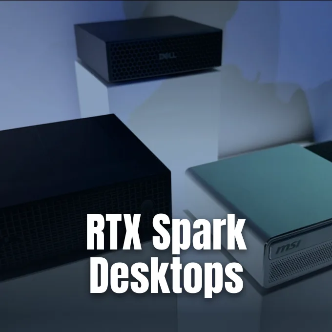
The upcoming Nvidia Rubin platform brings fifth-generation tensor units designed for reasoning models and modern AI factories. Nvidia Rubin blends narrow NVFP4 and FP8 math into streaming multiprocessors, pairing matrix units with special function hardware to speed up attention steps and sparse compute paths. A standalone Nvidia Rubin GPU features a 50-petaflops Transformer Engine driven by NVFP4 execution. In the rack-scale Vera Rubin NVL72 system, collective matrix units scale to 3,600 petaflops of NVFP4 inference throughput [2]. Server hardware also supports desktop systems, including Nvidia RTX Spark desktop hardware configured for local engineering tasks.
Matrix units also speed up scientific data tasks outside machine learning. In a 2023 paper in the Journal of Computational Science, researchers K. Fujita, T. Yamaguchi, Y. Kikuchi, T. Ichimura, M. Hori, and M. Lalith showed how TensorFloat-32 units speed up seismic cross-correlation math. By shaping data pipelines to match hardware matrix sizes, the team reached 54 teraflops on an Nvidia Ampere A100 GPU and 191 teraflops on an Nvidia Hopper H100 GPU, gaining a 3.6-fold speedup over baseline matrix math. Their findings showed that observational geophysics codes gain real speed when teams frame time-series math as dense matrix products [8].
Software Libraries for Matrix Math
Developers rarely program matrix units through raw assembly commands. Instead, Nvidia CUDA provides matrix tools through the Warp Matrix Multiply and Accumulate API, letting programmers load small matrix fragments into registers, run fused math across a warp of 32 threads, and write results back to memory. This abstraction hides hardware details from engineers [1, 9].
Higher in the software stack, specialized libraries optimize linear algebra routines for real-world deployments. Libraries like Nvidia cuDNN supply tuned convolution and attention routines, while Nvidia cuBLAS provides linear algebra subprograms accelerated by matrix units [1, 9]. For multi-GPU scaling, the Nvidia NCCL library coordinates communication across cluster nodes, ensuring matrix data moves between chips without stalling compute units. Developers writing in PyTorch or JAX call these routines automatically without writing custom GPU code [1]. Software ecosystems also extend these hardware capabilities to desktop workstations, connecting developer workflows with tools optimizing RTX 50 series workflows for rapid model prototyping.
Inference optimization software improves hardware use through layer fusion and quantization. Tools like Nvidia TensorRT and NeMo Framework compress models for serving, using 8-bit and 4-bit precision modes without hurting accuracy [1, 2]. These compilers ensure data center systems keep high utilization during production workloads [2].
Why Modern AI Relies on Tensor Cores
Modern generative models require compute speed that general processor designs cannot provide. Training massive mixture-of-experts systems, such as GPT-MoE-1.8T, requires running quadrillions of math steps across hundreds of billions of text tokens. Without hardware designed to compute dense matrix tiles in single clock ticks, training such models would demand impractical electrical power and huge server footprints [2, 3].
The efficiency advantages extend beyond frontier model training to real-time inference and local execution. When companies run reasoning agents or chat systems, latency per output token decides usability. By running matrix passes in FP4 or FP8 precision, fifth-generation tensor units reduce memory bottlenecks, letting models generate answers in milliseconds [2, 3]. Because smaller data needs fewer memory reads, servers use less power per query, making widespread enterprise AI deployment practical [2]. Switching bit formats between training and serving helps operators get the most value from expensive server hardware [3].
Matrix acceleration has also reshaped consumer graphics and real-time rendering. Neural rendering pipelines use tensor hardware to build high-resolution images from lower-resolution frames, predicting lighting and temporal details with deep learning models. Outside official developer channels, community enthusiasts test these rendering boundaries, as when modders inject DLSS into unsupported games to evaluate neural upscaling performance on consumer hardware. From supercomputers analyzing seismic data to desktop GPUs rendering games, hardware matrix units have become a vital base of modern computing [3, 8].
- WEBSITE NVIDIA. (2023). NVIDIA Volta AI Architecture. [Article Link]
- WEBSITE NVIDIA. (2026). NVIDIA Tensor Cores: Versatility for HPC & AI. [Article Link]
- WEBSITE Exxactcorp. (2025). Comparing Blackwell vs Hopper | B300 & B200 vs H200 & H100. [Article Link]
- WEBSITE Wikipedia contributors. (n.d.). Volta (microarchitecture). [Article Link]
- ACADEMIC JOURNAL Fasi, M., Higham, N. J., Mikaitis, M., & Pranesh, S. (2021). Numerical behavior of NVIDIA tensor cores. PeerJ Computer Science, 7, e330. [Article Link]
- ACADEMIC JOURNAL Khattak, F. A., & Mikaitis, M. (2026). Accurate Models of NVIDIA Tensor Cores. ACM Transactions on Architecture and Code Optimization, 23(3), 1–25. [Article Link]
- ACADEMIC JOURNAL Choquette, J., Gandhi, W., Giroux, O., Stam, N., & Krashinsky, R. (2021). NVIDIA A100 Tensor Core GPU: Performance and Innovation. IEEE Micro, 41(2), 29–35. [Article Link]
- ACADEMIC JOURNAL Fujita, K., Yamaguchi, T., Kikuchi, Y., Ichimura, T., Hori, M., & Lalith, M. (2023). Calculation of cross-correlation function accelerated by TensorFloat-32 Tensor Core operations on NVIDIA’s Ampere and Hopper GPUs. Journal of Computational Science, 68, 101986. [Article Link]
- REPORT Ejaz, S. T. (2026). Tensor Core Matrix Multiplication on the NVIDIA T4: A WMMA FP16 GEMM with Double Buffering, Compared Against cuBLAS. Zenodo. [Article Link]


