




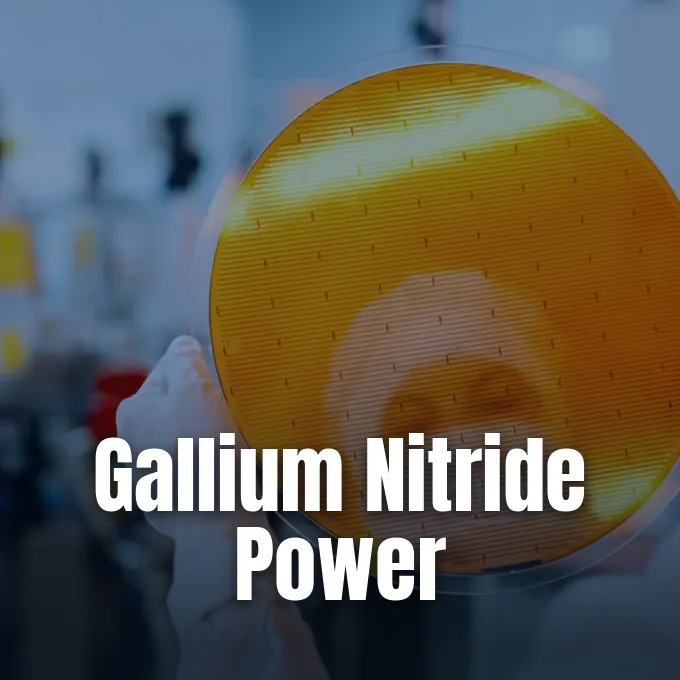
Gallium nitride is a wide-bandgap semiconductor that handles high voltages and conducts electrical current with far less heat than traditional silicon. It switches current faster [1]. That switching speed cuts energy losses in mobile power adapters, industrial motor controllers, and wireless communications equipment. Engineers use the compound to produce compact power supplies that stay cool while delivering high electrical wattage to consumer devices. Electrical grids and cloud data centers face increasing energy demands each year. The material steadily replaces aging silicon components to improve conversion efficiency in modern power electronics [4].
What Is Gallium Nitride?
Gallium nitride, known chemically as GaN, is a binary III/V direct bandgap semiconductor composed of gallium and nitrogen atoms organized in a wurtzite crystal structure. Pure crystals are hard, registering a Knoop hardness of 14.21 GPa, and resist mechanical cracking during high-temperature operations. In semiconductor physics, the bandgap represents the energy barrier that electrons must cross to jump from the valence band into the conduction band to conduct electricity. Silicon features an energy bandgap of roughly 1.1 eV. By contrast, GaN provides a wide bandgap of 3.4 eV [1]. This wider gap allows the material to handle high electrical fields without breaking down.
The chemical compound remains stable in environments exposed to ionizing radiation, which makes it suitable for solar cell arrays deployed on space satellites. In 1999, researchers at the U.S. Army Research Laboratory measured high-field electron velocity in GaN, recording a peak steady-state velocity of 1.9×10^7 cm/s with a transit time of 2.5 picoseconds under an electric field of 225 kV/cm. These physical characteristics yield a high Johnson’s figure of merit, and allow devices to operate at temperatures reaching 400 °C, while silicon begins to fail near 150 °C [1].
High thermal stability lets engineers design power hardware that functions without heavy cooling assemblies. Because GaN withstands larger internal electric fields, power devices can be built with thinner layers and tighter dimensions. Current flows through the lattice with minimal resistance. This physical resilience forms the core foundation for modern solid-state electronics [1].
Physical Properties and Bandgap Structure
Aluminium gallium nitride, known as AlGaN, is an alloy of aluminium nitride and GaN whose direct bandgap can be adjusted from 3.4 eV up to 6.2 eV by modifying the aluminium mole fraction. This broad bandgap span allows manufacturers to produce ultraviolet detectors and light-emitting diodes that emit light at wavelengths as short as 210 nm [15]. Mixing GaN with indium nitride creates indium gallium nitride, or InGaN, which spans an absorption band from 0.69 eV to 3.4 eV. The ratio of indium to gallium in commercial optoelectronics usually ranges between 0.02 to 0.98 and 0.3 to 0.7 [16]. Research into semiconductor interfaces also explores how integrating delicate 2D materials into devices provides distinct electronic transport channels.
Indium gallium nitride can also be formed into nanoscale column structures to improve light emission and energy conversion [16]. In a 2012 study released on the preprint server arXiv, researchers S. Keating, M. G. Urquhart, D. V. P. McLaughlin, and J. M. Pearce synthesized InGaN films on amorphous silicon dioxide using plasma-enhanced evaporation. The authors reported that lower substrate temperatures produced thinner and more tightly packed nanocolumns with reduced void fractions, though their findings remain an unreviewed preprint [17]. A companion preprint by McLaughlin and Pearce developed analytical models for optical functions in InGaN thin films to assess their efficiency in photovoltaic solar cells [18].
Alloy composition controls the exact energy levels inside group III nitride semiconductors [16]. When layers of AlGaN and GaN meet, the natural polar charges generate thin electron layers that conduct current smoothly. These structural features allow engineers to tune optical and electrical behavior on a single wafer [15].
History of the Blue LED Breakthrough
Russian chemist Dmitri Mendeleev first predicted the existence of gallium in 1871, and French chemist Paul-Émile Lecoq de Boisbaudran discovered the element in Paris in 1875. The earliest synthesis of polycrystalline gallium nitride occurred in 1932 at the George Herbert Jones Laboratory by passing ammonia gas over liquid gallium at temperatures between 900 °C and 1,000 °C [2]. Researchers Robert Juza and Harry Hahn conducted another synthesis in 1938 [1]. Decades later, in 1969, H. P. Maruska and J. J. Tietjen deposited single-crystal GaN films on sapphire substrates using hydride vapor phase epitaxy. In 1972, J. I. Pankove, E. A. Miller, and J. E. Berkeyheiser built a GaN device that produced blue luminescence, but its low efficiency prevented commercial adoption [2].
The breakthrough that changed consumer lighting came during the early 1990s in Japan. In 1991, researcher Shuji Nakamura at Nichia Chemical, working with Nagoya University scientists Isamu Akasaki and Hiroshi Amano, patented a method to manufacture high-brightness blue light-emitting diodes. By doping GaN with higher amounts of magnesium, the team achieved efficient p-type conductivity, demonstrating practical blue LEDs in 1993. Blue emission was the missing piece needed to create full-color RGB displays and white solid-state lighting. Display engineers later expanded these optical concepts into consumer television screens, where technologies like OLED and QLED display panels compete on contrast and brightness. Akasaki, Amano, and Nakamura shared the 2014 Nobel Prize in Physics for their work [2].

Why Gallium Nitride Outperforms Silicon
Silicon has powered computing for decades, but it approaches physical boundaries in high-power applications [3]. When silicon MOSFETs switch high voltages, internal electrical resistance converts valuable electrical power into waste heat [4]. In 1994, researcher M. A. Khan and his team discovered that growing a thin layer of AlGaN over gallium nitride created a two-dimensional electron gas, abbreviated as 2DEG. The electron mobility measured in this interface layer was 12 times higher at room temperature than in standard bulk GaN [2]. This electron gas produces a low on-resistance, known in power engineering as RDS(on), so electrical current travels through the transistor channel with minimal conduction loss [3].
Devices built from GaN switch electrical states much faster than silicon transistors because they operate as majority-carrier components. This majority-carrier structure gives the intrinsic body diode a reverse recovery charge, designated (QRR), of zero. In conventional silicon switches, stored minority charges must discharge during every switching cycle, creating switching delays and wasting energy. GaN transistors eliminate this discharge penalty, switching hundreds of volts in nanoseconds. Low gate-drain capacitance further accelerates voltage transitions [3]. These electrical characteristics allow power supplies to operate at high frequencies with minimal power loss.
Higher switching speed directly alters hardware dimensions. Because circuits cycle power faster, magnetic inductors store energy in smaller increments. Transformers shrink in physical size. Engineers pack more power into smaller enclosures without causing thermal failure [4].



Solving the Normally-On Transistor Hurdle
Early GaN transistors suffered from a major operational limitation despite their electrical benefits [3]. Standard high-electron-mobility transistors, first explored by Takashi Mimura in 1975 and commercialized for radio frequencies by Eudyna Device in 2004, were depletion-mode switches [2]. Depletion-mode devices are “normally on,” meaning they conduct electricity when the gate voltage is at zero volts. Power distribution systems demand enhancement-mode transistors that remain “normally off” by default [3]. If a control circuit loses power or fails, normally-on switches remain open, which creates high-current shorts that can destroy downstream electronics [4].
Engineers devised several methods to overcome this flaw, including fluorine ion treatment and recessed gate designs [1]. At MIT, associate professor Tomás Palacios, Anantha Chandrakasan, and doctoral researchers Bin Lu and Omair Saadat altered epitaxial recipes to produce normally-off GaN switches. “This is a once-in-a-lifetime opportunity to change electronics and to really make an impact on how energy is used in the world,” Palacios said. Lu explained how fabricating these devices in standard silicon manufacturing facilities reduced production expenses. “Basically, we are fabricating our advanced GaN transistors and circuits in conventional silicon foundries, at the cost of silicon,” Lu said [4].
In 2010, former International Rectifier executive Alex Lidow founded Efficient Power Conversion, known as (EPC), to bring enhancement-mode GaN to market. EPC launched transistors such as the EPC1001, a 100-volt device with an on-resistance of 5.6 milliohms grown directly on silicon wafers. The transistor operated with a gate threshold around 1.5 volts and achieved full enhancement at 5 volts. This voltage profile allowed the device to interface with existing gate drivers. Silicon-compatible enhancement-mode switches cleared the way for commercial adoption across consumer and industrial sectors [3].
Why Consumer Chargers Adopted GaN
Consumer electronics adapters became the first mass-market application for gallium nitride semiconductors [5]. At MIT spinout Cambridge Electronics, researchers used GaN transistors to develop a prototype laptop power adapter measuring 1.5 cubic inches, and it was the smallest laptop power supply built at the time. Traditional laptop chargers rely on silicon transistors that switch at relatively low frequencies, requiring large capacitors and heavy copper transformers to filter electricity [4]. GaN switches operate at frequencies above 500 kHz, so power supplies use magnetic components that are up to 60 percent smaller [6].
Hardware manufacturers like Anker and RAVPower brought compact chargers to retail shelves, cutting adapter volume in half while delivering 30 watts to 65 watts of power over USB-C [5]. Texas Instruments developed integrated AC-to-DC converters like the UCG28826, which combines GaN HEMTs, gate drivers, and circuit protections into a single package. By integrating the gate driver, engineers eliminate parasitic loop inductance that causes voltage overshoot. These integrated power stages reach conversion efficiencies above 95 percent, and wall adapters stay cool during fast charging sessions [6].
Lower operating temperatures remove the need for internal metal heatsinks, which further decreases adapter weight and volume [4]. Consumer accessories become easier to transport. Because less power is lost as thermal waste, devices charge faster with less energy drawn from wall outlets. Large-scale semiconductor production continues to narrow the price gap between GaN chargers and older silicon models [5].
Performance in Electric Vehicles
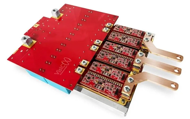
Electric vehicles require efficient power conversion to maximize driving distance from onboard battery packs. The traction inverter serves as the central bridge between the battery and the electric motor, which converts direct current into three-phase alternating current. Traditional electric car inverters use silicon IGBTs or silicon carbide modules, but automotive-grade gallium nitride devices deliver superior switching efficiency. A reference traction inverter developed with VisIC V22TC65S1A1 power switches achieved a peak efficiency of 99.3% at a switching frequency of 40 kHz. That 800-volt three-level design produced a power density of 50 kW per liter and weighed 2.5 kilograms [7].
Automotive engineers apply GaN components to multiple vehicle sub-systems, including on-board battery chargers and high-to-low DC/DC converters. Research teams from Toyota and Nagoya University demonstrated these efficiency gains in an experimental vehicle, and confirmed lower thermal dissipation and smaller component packaging [7]. Lower power losses reduce the size of liquid cooling loops, and sheds vehicle curb weight. In October 2026, German chipmaker Infineon announced an investment of €1.1 billion into its production facility in Villach, Austria, supported by the European Union Chips Act to expand automotive and industrial GaN chip manufacturing [8].
Infineon manufactures GaN power semiconductors on 300-millimeter wafers, which yield 2.3 times more chips per wafer than older 200 mm production lines. Thomas Neyer, senior vice president of Infineon’s GaN business line, described the engineering challenges of managing thermal expansion mismatch between silicon wafers and GaN crystal layers. “For GaN on a 300 mm Si wafer, this stress is as high as four elephants (5 tons each) sitting on a 1 Euro Cent coin,” Neyer said. Overcoming that mechanical strain enables high-volume manufacturing with lower per-unit costs [9].
Military Radar and Integrated Circuits
Phased-array radar systems represent a demanding proving ground for gallium nitride semiconductors [11]. In 2011, Northrop Grumman tested high-power transmit/receive modules for 180 days of continuous operation using long-pulse waveforms that simulated tactical radar workloads. Steve McCoy, vice president in the company’s Electronic Systems sector, said the evaluation verified technology readiness for next-generation active electronically scanned array radars [10]. In 2018, the U.S. Army awarded Lockheed Martin a contract modification to insert GaN devices into the AN/TPQ-53 counterfire radar, to replace older AN/TPQ-36 and AN/TPQ-37 systems [12]. Program director Rick Herodes said GaN increased transmission power, which improved radar illumination and detection range against artillery and drones [11].
Military systems benefit from GaN because its high breakdown voltage allows radar transmitters to emit powerful RF pulses from compact antenna arrays [11]. Defense contractor Thales Group deployed more than 50,000 GaN transmitters on operational radars, including its Ground Master 400 system. Swedish defense company Saab integrated GaN into its Gripen fighter radar systems, while Israel’s ELTA Systems used the material in its ELM-2084 radar. High thermal tolerance keeps these phased arrays operational in harsh operating environments without bulky refrigeration gear [1].
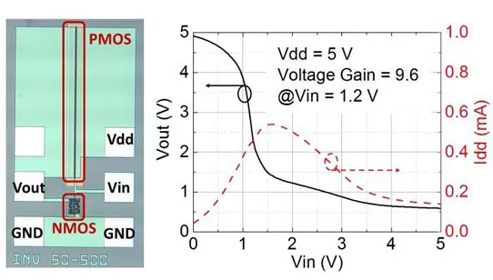
Future development centers on complementary logic. In 2016, Rongming Chu and a team at HRL Laboratories built the first GaN CMOS inverter circuits, which paired NMOS and PMOS transistors on sapphire substrates. That work demonstrated that GaN logic circuits could control power switches on the same chip without parasitic interconnect delays [13]. In 2026, researchers led by C. F. C. Chang, Debdeep Jena, and Huili Grace Xing reported in Nature Electronics that polarization-induced two-dimensional hole gases at gallium nitride and aluminium nitride interfaces reached mobilities of 2,000 cm2/V-s at cryogenic temperatures. This discovery highlights potential applications for GaN control circuits in quantum computing hardware [14].
- WEBSITE Wikipedia contributors. (2026). Gallium nitride. Wikipedia, The Free Encyclopedia. [Article Link]
- ONLINE NEWS Ahmad, M. (2023). A brief history of gallium nitride (GaN) semiconductors. EDN. [Article Link]
- ONLINE NEWS Davis, S. (2010). Enhancement Mode Gallium Nitride MOSFET Delivers Impressive Performance. Electronic Design. [Article Link]
- ONLINE NEWS Matheson, R. (2015). Making the new silicon: Gallium nitride electronics could drastically cut energy usage. Phys.org. [Article Link]
- WEBSITE Kuek, Z. (2022). Apple 30W Compact GaN Charger. ManMade Cycle. [Article Link]
- WEBSITE Texas Instruments. (2026). Gallium nitride (GaN) technology and power applications. TI.com. [Article Link]
- ONLINE NEWS Azcuénaga, D. de. (2025). GaN Advances EV Power Design. Power Electronics News. [Article Link]
- ONLINE NEWS Broersma, M. (2026). Infineon Plans €1.1bn Upgrade For Gallium-Nitride Chip Plant. Silicon UK. [Article Link]
- ONLINE NEWS Emilio, M. D. P. (2024). Infineon Advances GaN Technology with 300 mm Wafer Production. Power Electronics News. [Article Link]
- ONLINE NEWS Space War Editorial Team. (2011). Gallium Nitride-Based Modules Set New 180-Day Standard For High Power Operation. Space War. [Article Link]
- ONLINE NEWS Browne, J. (2018). GaN Extends Range of Army’s Q-53 Radar System. Microwaves & RF. [Article Link]
- PRESS RELEASE Lockheed Martin Corporation. (2018). U.S. Army Awards Lockheed Martin Contract Extending AN/TPQ-53 Radar Range. Lockheed Martin. [Article Link]
- ONLINE NEWS Cooke, M. (2016). HRL Laboratories claims first gallium nitride CMOS transistor fabrication. Semiconductor Today. [Article Link]
- ACADEMIC JOURNAL Chang, C. F. C., Dill, J. E., Zhang, Z., Chen, J., Pieczulewski, N., Bader, S. J., Ayala Valenzuela, O. E., Crooker, S. A., Balakirev, F. F., McDonald, R. D., Encomendero, J., Muller, D. A., Giustino, F., Jena, D., & Xing, H. G. (2026). High-mobility holes in gallium nitride and their quantum oscillations. Nature Electronics, 9(4), 346-357. [Article Link]
- WEBSITE Wikipedia contributors. (2026). Aluminium gallium nitride. Wikipedia, The Free Encyclopedia. [Article Link]
- WEBSITE Wikipedia contributors. (2026). Indium gallium nitride. Wikipedia, The Free Encyclopedia. [Article Link]
- PREPRINT Keating, S., Urquhart, M. G., McLaughlin, D. V. P., & Pearce, J. M. (2012). Effects of Substrate Temperature on Indium Gallium Nitride Nanocolumn Crystal Growth. arXiv. [Article Link]
- PREPRINT McLaughlin, D. V. P., & Pearce, J. M. (2012). Analytical Model for the Optical Functions of Indium Gallium Nitride with Application to Thin Film Solar Photovoltaic Cells. arXiv. [Article Link]


